PCF2119VU-2 Ver la hoja de datos (PDF) - Philips Electronics
Número de pieza
componentes Descripción
Fabricante
PCF2119VU-2 Datasheet PDF : 68 Pages
| |||
Philips Semiconductors
LCD controllers/drivers
Product specification
PCF2119X
6 PAD INFORMATION
The identification of each pad and its location is given in Chapter 18.
6.1 Pad functions
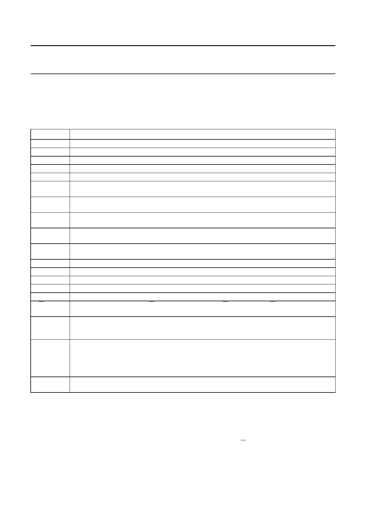
Table 1 Pad function description
SYMBOL
VDD1
VDD2, VDD3
VSS1
VSS2
VLCD1
VLCD2
VLCDSENSE
E
T1 to T3
R1 to R18;
R17DUP
C1 to C80
SCL
POR
PD
SDA
R/W
RS
DB0 to DB7
OSC
DESCRIPTION
Logic supply voltage.
High voltage generator supply voltages (always put VDD2 = VDD3).
This is the ground pad for all except the high voltage generator.
This is the ground pad for the high voltage generator.
This input is used for the generation of the LCD bias levels.
This is the VLCD output pad if VLCD is generated internally then pad VLCD2 must be connected to VLCD1.
The pad must be left open-circuit when VLCD is generated externally.
This input (VLCD) is used for the voltage multiplier’s regulation circuitry. This pad must be connected to
VLCD2 when using internal LCD supply and to VLCD1 and VLCD2 when using external LCD supply.
The data bus clock input is set HIGH to signal the start of a read or write operation; data is clocked in
or out of the chip on the negative edge of the clock; note 1.
These are three test pads. T1 and T2 must be connected to VSS1; T3 is left open-circuit and is not user
accessible.
LCD row driver outputs R1 to R18; these pads output the row select waveforms to the display;
R17 and R18 drive the icons. R17 has two pads R17 and R17DUP.
LCD column driver outputs C1 to C80.
I2C-bus serial clock input; note 1.
External power-on reset input.
PD selects the chip power-down mode; for normal operation PD = 0.
I2C-bus serial data input/output; note 1.
This is the read/write input. R/W selects either the read (R/W = 1) or write (R/W = 0) operation. This
pad has an internal pull-up resistor.
The RS input selects the register to be accessed for read and write. RS = 0, selects the instruction
register for write and the busy flag and address counter for read. RS = 1, selects the data register for
both read and write. This pad has an internal pull-up resistor.
The 8-bit bidirectional data bus (3-state) transfers data between the system controller and the
PCF2119x. DB7 may be used as the busy flag, signalling that internal operations are not yet
completed. In 4-bit operations the 4 higher order lines DB7 to DB4 are used; DB3 to DB0 must be left
open-circuit. Data bus line DB3 has an alternative function (SA0), when selected this is the I2C-bus
address pad. Each data line has its own internal pull-up resistor; note 1.
Oscillator or external clock input. When the on-chip oscillator is used this pad must be connected to
VDD1.
Note
1. When the I2C-bus is used, the parallel interface pad E must be at logic 0. In the I2C-bus read mode DB7 to DB4 and
DB2 to DB0 should be connected to VDD1 or left open-circuit.
a) When the parallel bus is used, pads SCL and SDA must be connected to VSS1 or VDD1; they must not be left
open-circuit.
b) If the 4-bit interface is used without reading out from the PCF2119x (i.e. R/W is set permanently to logic 0), the
unused ports DB0 to DB4 can either be set to VSS1 or VDD1 instead of leaving them open-circuit.
2003 Jan 30
6
Share Link: 