PCA9512BD Ver la hoja de datos (PDF) - NXP Semiconductors.
Número de pieza
componentes Descripción
Fabricante
PCA9512BD Datasheet PDF : 27 Pages
| |||
NXP Semiconductors
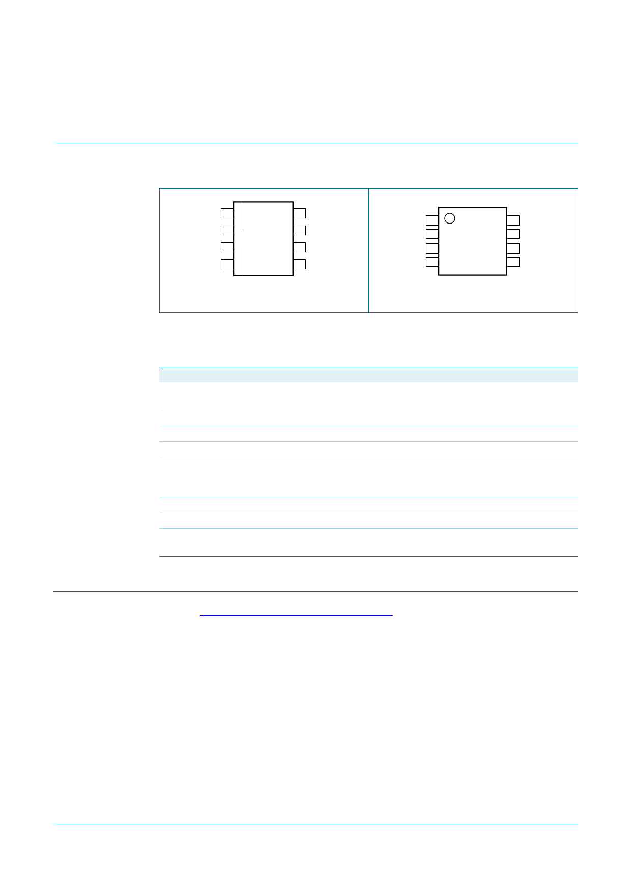
7. Pinning information
7.1 Pinning
PCA9512A; PCA9512B
Level shifting hot swappable I2C-bus and SMBus bus buffer
VCC2 1
8 VCC
SCLOUT 2 PCA9512AD 7 SDAOUT
SCLIN 3 PCA9512BD 6 SDAIN
GND 4
5 ACC
002aab789
Fig 2. Pin configuration for SO8
VCC2 1
SCLOUT 2
SCLIN 3
GND 4
PCA9512ADP
PCA9512BDP
8 VCC
7 SDAOUT
6 SDAIN
5 ACC
002aab790
Fig 3. Pin configuration for TSSOP8
7.2 Pin description
Table 4. Pin description
Symbol Pin Description
VCC2
1
Supply voltage for devices on the card I2C-bus. Connect pull-up resistors
from SDAOUT and SCLOUT to this pin.
SCLOUT 2
serial clock output to and from the SCL bus on the card
SCLIN
3
serial clock input to and from the SCL bus on the backplane
GND
4
ground supply; connect this pin to a ground plane for best results.
ACC
SDAIN
5
CMOS threshold digital input pin that enables and disables the rise time
accelerators on all four SDAn and SCLn pins. ACC enables all accelerators
when set to VCC2, and turns them off when set to GND.
6
serial data input to and from the SDA bus on the backplane
SDAOUT 7
serial data output to and from the SDA bus on the card
VCC
8
supply voltage; from the backplane, connect pull-up resistors from SDAIN
and SCLIN to this pin.
8. Functional description
Refer to Figure 1 “Block diagram of PCA9512A/B”.
Both the PCA9512A and PCA9512B use identical silicon (PCN201012007F dated
13 Dec 2010), so the PCA9512B will be discontinued in the near future and is not
recommended for new designs. Customers should continue using the PCA9512A or move
to the PCA9512A during the next refresh if they are currently using the PCA9512B.
Description of the PCA9512A operation applies equally to the PCA9512B for the
remainder of this data sheet.
8.1 Start-up
When the PCA9512A is powered up, either VCC or VCC2 may rise first, within a short time
of each other and either may be more positive or they may be equal, however the
PCA9512A will not leave the undervoltage lockout or initialization state until both VCC and
VCC2 have gone above 2.5 V. If either VCC or VCC2 drops below 2.0 V it will return to the
undervoltage lockout state.
PCA9512A_PCA9512B
Product data sheet
All information provided in this document is subject to legal disclaimers.
Rev. 6 — 1 March 2013
© NXP B.V. 2013. All rights reserved.
5 of 27
Share Link: 