PCA9509 Ver la hoja de datos (PDF) - NXP Semiconductors.
Número de pieza
componentes Descripción
Fabricante
PCA9509 Datasheet PDF : 24 Pages
| |||
NXP Semiconductors
PCA9509
Level translating I2C-bus/SMBus repeater
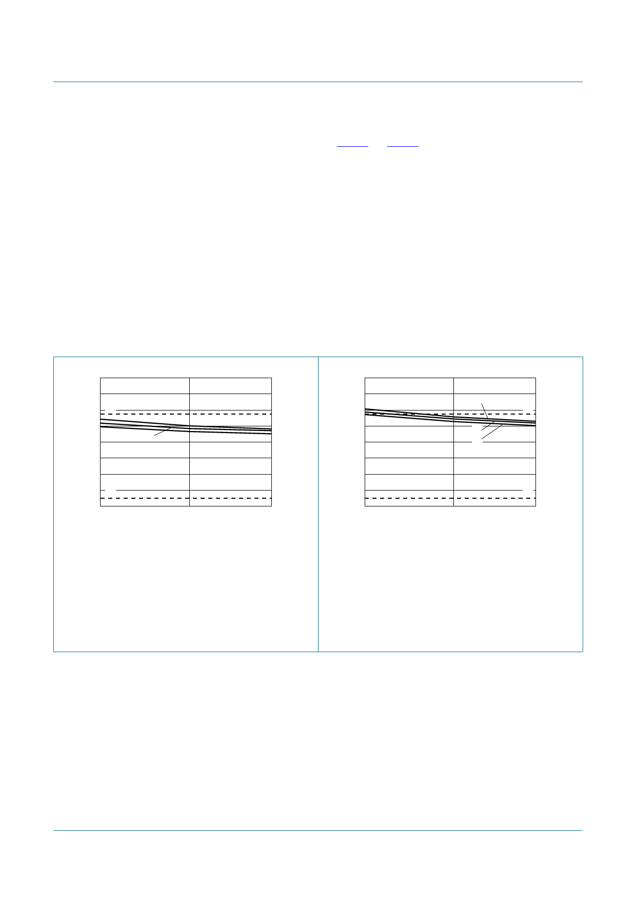
[2] If the PCA9509 is not being enabled or disabled, the VCC(A) minimum is 0.95 V with a corresponding decrease in the IIL, which will drop
below the minimum specification of 450 A at cold temperature (see Figure 8 and Figure 9). This will not significantly change the rise
and fall times of the signals on port A since the IIL value represents the current source pull-up current, so a lower current into the same
capacitance results in a slower rise time and a longer transition time in general, however since the lower current is also associated with
a lower voltage swing the delay is somewhat compensated. The key point of the graphs is that the current has a temperature
dependence, and the output driver will also have the same temperature dependency so that the output offset of ~200 mV on port A is
nearly temperature independent. Even though the IIL parameter indicates that at VCC(A) of 0.95 V the PCA9509 can only sink up to
400 A instead of 450 A at cold temperature, the output is designed to be somewhat resistive such that under nominal conditions
(1.1 V) the current source pull-up sources 1 mA and the output pull-down sinks the 1 mA at ~200 mV, so as the current source current
decreases the output pull-down resistance increases in order to maintain the offset.
[3] VIL specification is for the falling edge seen by the port A input. VILc is for the static LOW levels seen by the port A input resulting in
port B output staying LOW.
[4] The port A current source has a typical value of about 1 mA, but varies with both VCC(A) and VCC(B). Below VCC(A) of about 0.7 V the
port A current source current drops to 0 mA. The current source current dropping across the internal pull-down driver resistance of
about 200 defines the VOL.
[5] As long as the chip ground is common with the input ground reference the driver resistance may be as large as 120 . However, ground
offset will rapidly decrease the maximum allowed driver resistance.
[6] Guaranteed by design.
0
IIL
(mA)
−0.4 (1)
−0.8
(2)
(3)
(4)
002aae733
−1.2
(5)
−1.6
−40
25
85
Tamb (°C)
Pins under test = An pins
(1) High limit
(2) Maximum
(3) Mean
(4) Minimum
(5) Low limit
Fig 8. LOW-level input current as a function of
temperature; VCC(A) = 1.0 V
0
IIL
(mA)
−0.4
−0.8
002aae734
(2)
(1)
(3)
(4)
−1.2
−1.6
−40
(5)
25
85
Tamb (°C)
Pins under test = An pins
(1) High limit
(2) Maximum
(3) Mean
(4) Minimum
(5) Low limit
Fig 9. LOW-level input current as a function of
temperature; VCC(A) = 0.95 V
PCA9509
Product data sheet
All information provided in this document is subject to legal disclaimers.
Rev. 7 — 4 November 2014
© NXP Semiconductors N.V. 2014. All rights reserved.
9 of 24
Share Link: 