PCA9509D(2009) Ver la hoja de datos (PDF) - NXP Semiconductors.
Número de pieza
componentes Descripción
Fabricante
PCA9509D Datasheet PDF : 19 Pages
| |||
NXP Semiconductors
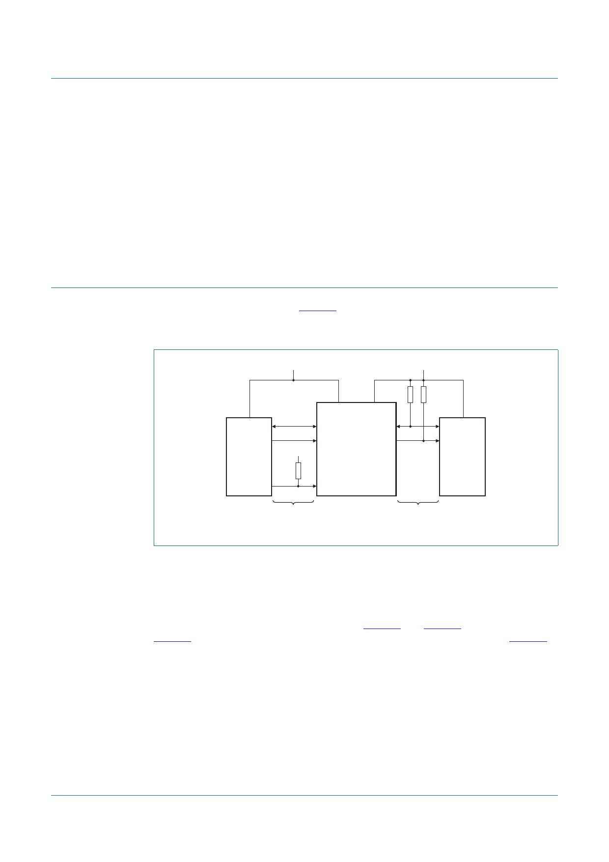
PCA9509
Level translating I2C-bus/SMBus repeater
SCL
SDA
9th clock pulse
acknowledge
Fig 6. Bus B SMBus/I2C-bus waveform
002aab644
9th clock pulse
acknowledge
SCL
SDA
VOL of PCA9509
VOL of master
Fig 7. Bus A lower voltage waveform
002aac129
8. Limiting values
Table 3. Limiting values
In accordance with the Absolute Maximum Rating System (IEC 60134).
Symbol Parameter
Conditions
VCC(B)
VCC(A)
VI/O
supply voltage port B
supply voltage port A
voltage on an input/output pin
port A
port B; enable pin (EN)
II/O
II
Ptot
Tstg
Tamb
Tj
Tsp
input/output current
input current
total power dissipation
storage temperature
ambient temperature
junction temperature
solder point temperature
operating in free air
10 s max.
Min
−0.5
−0.5
−0.5
−0.5
-
-
-
−65
−40
-
-
Max Unit
+6.0 V
+6.0 V
+6.0 V
+6.0 V
±20 mA
±20 mA
100 mW
+150 °C
+85 °C
+125 °C
300 °C
PCA9509_5
Product data sheet
Rev. 05 — 10 July 2009
© NXP B.V. 2009. All rights reserved.
6 of 19
Share Link: 