PCA84C846 Ver la hoja de datos (PDF) - Philips Electronics
Número de pieza
componentes Descripción
Fabricante
PCA84C846 Datasheet PDF : 72 Pages
| |||
Philips Semiconductors
Microcontrollers for TV tuning
control and OSD applications
Preliminary specification
PCA84C646; PCA84C846
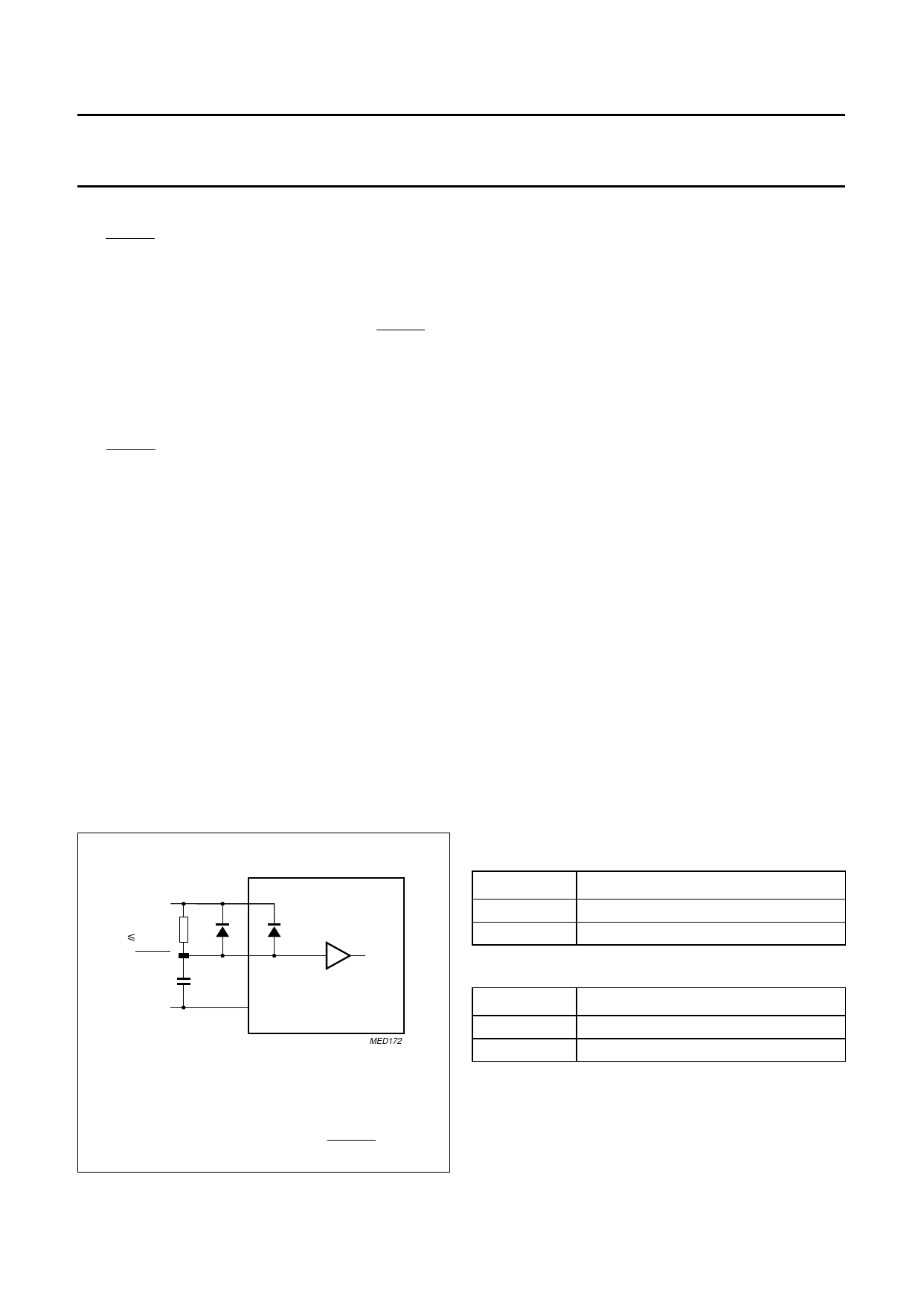
6 RESET
The RESET pin is used as an active LOW input to initialize
the microcontroller to a defined state.
A Power-on-reset can be generated by using the
RC-circuit as shown in Fig.3.
An active reset can be generated by driving the RESET pin
from an external logic device. Such an active reset pulse
should not fall off before VDD has reached its
fxtal-dependent minimum operating voltage.
6.1 Reset trip level
The RESET trip-voltage level is masked to 1.3 V in the
PCA84C646 and PCA84C846.
6.2 Reset status
• Derivative Registers status; for details see Table 40
• Program Counter: 00H
• Memory Bank: 00H
• Register Bank: 00H
• Stack Pointer: 00H
• All interrupts disabled
• Timer/event counter 1 stopped and cleared
• Timer prescaler modulo-32 (PS = 0)
• Timer flag cleared
• Serial I/O interface disabled (ESO = 0) and in slave
receiver mode
• Idle and Stop mode cleared.
7 ANALOG CONTROL
7.1 6 and 7-bit PWM outputs (PWM00 to PWM07)
The PCA84C646/PCA84C846 has eight PWM outputs for
analog controls of e.g. volume, balance, brightness and
saturation. These PWM outputs generate pulse patterns
with a repetition rate of 1⁄64 × fPWM or 1⁄128 × fPWM. The
analog value is determined by the ratio of the HIGH-time
and the repetition time. A DC voltage proportional to the
PWM control setting is obtained by means of an external
integration network (low-pass filter).
The eight PWM outputs are specified as follows:
• PWM00 to PWM03 outputs with 7-bit resolution
• PWM04 to PWM07 outputs with 6-bit resolution.
Figure 4 shows the block diagram of the 6-bit or 7-bit PWM
DAC. The polarity of the PWM0n output is selected as
shown in Table 2 by the polarity control bit P6LVL/P7LVL
(Derivative Register 23; see Table 25).
The PWM0n output shares the pin with a DP0n I/O line
under control of a PWMnE enable bit; for selection see
Table 3.
Figure 5 shows the 6 and 7-bit PWM0n output patterns
(non-inverted; P6LVL/P7LVL = 0).
The HIGH-time of a PWM0n output is
tHIGH = [PWMnDL] × t0
where:
[PWMnDL] = the contents of PWMn data latch
(n = 0 to 7; Derivative Register 10 to 17; see Table 40)
t0 = 1/fPWM; fPWM = 1⁄3 × fxtal.
V DD
R RESET
( 100 kΩ)
RESET
C RESET
V SS
(1)
internal reset
PCA84C646/846
MED172
(1) To avoid overload of the internal diode, an external
diode should be added in parallel if CRESET > 0.2 µF.
Table 2 Polarity selection for the PWM0n output
P6LVL/P7LVL
1
0
POLARITY
inverted
not inverted
Table 3 Selection of pin function: DP0n/PWM0n (note 1)
PWMnE
1
0
FUNCTION
PWM0n output
DP0n I/O
Note
1. n = 0 to 7.
Fig.3 External components for RESET pin.
1995 Jun 15
8
Share Link: 