PC410L0NIP0F Ver la hoja de datos (PDF) - Sharp Electronics
Número de pieza
componentes Descripción
Fabricante
PC410L0NIP0F Datasheet PDF : 13 Pages
| |||
PC410L0NIP0F Series
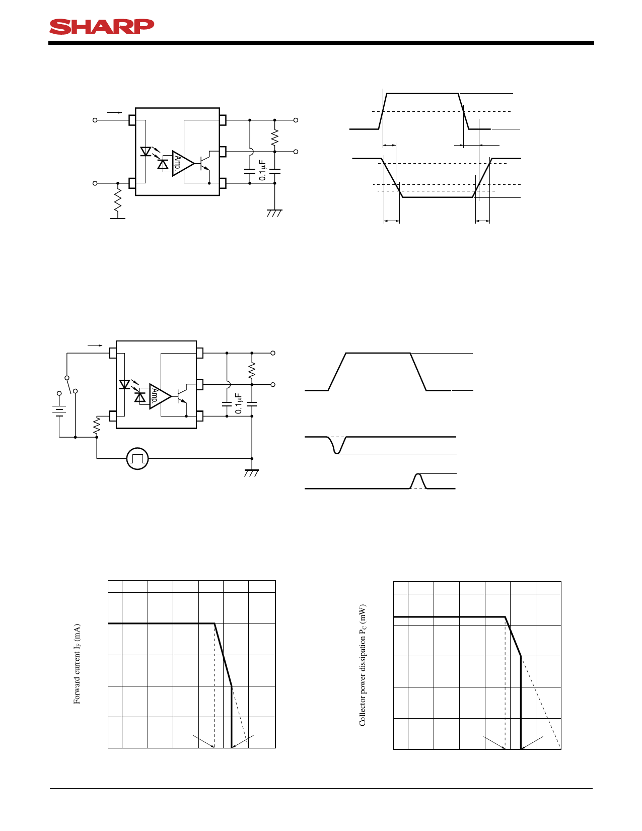
Fig.1 Test Circuit for Propagation Delay Time and Rise Time, Fall Time
Pulse input
IF
1
3
47Ω
IF
6
5V
350Ω
tPHL
5
VO
90%
CL
VO
4
10%
tf
*CL includes the probe
and wiring capacitance.
7.5mA
3.75mA
0mA
tPLH
5V
1.5V
VOL
tr
Fig.2 Test Circuit for Instantaneous Common Mode Rejection Voltage
GL SW IF
1
B
A
3
VCM
+
−
6
5V
350Ω
5
VO
VCM
CL
4
VO
(IF=0)
*CL includes the probe
VO
and wiring capacitance. (IF=5mA)
1kV
0V
5V
When the switch for
VO(MIN.) LED sets to A
VO(MAX.) When the switch for
VOL
LED sets to B
Fig.3 Forward Current vs. Ambient
Temperature
25
20
15
10
5
0
−40 −25
70
85
0 25 50 75 100 125
Ambient temperature Ta (°C)
Fig.4 Collector Power Dissipation vs.
Ambient Temperature
100
85
80
60
40
20
0
−40 −25
70
85
0 25 50 75 100 125
Ambient temperature Ta (°C)
Sheet No.: D2-A04802FEN
6
Share Link: 