74LV259D Ver la hoja de datos (PDF) - Philips Electronics
Número de pieza
componentes Descripción
Fabricante
74LV259D Datasheet PDF : 14 Pages
| |||
Philips Semiconductors
8-bit addressable latch
Product specification
74LV259
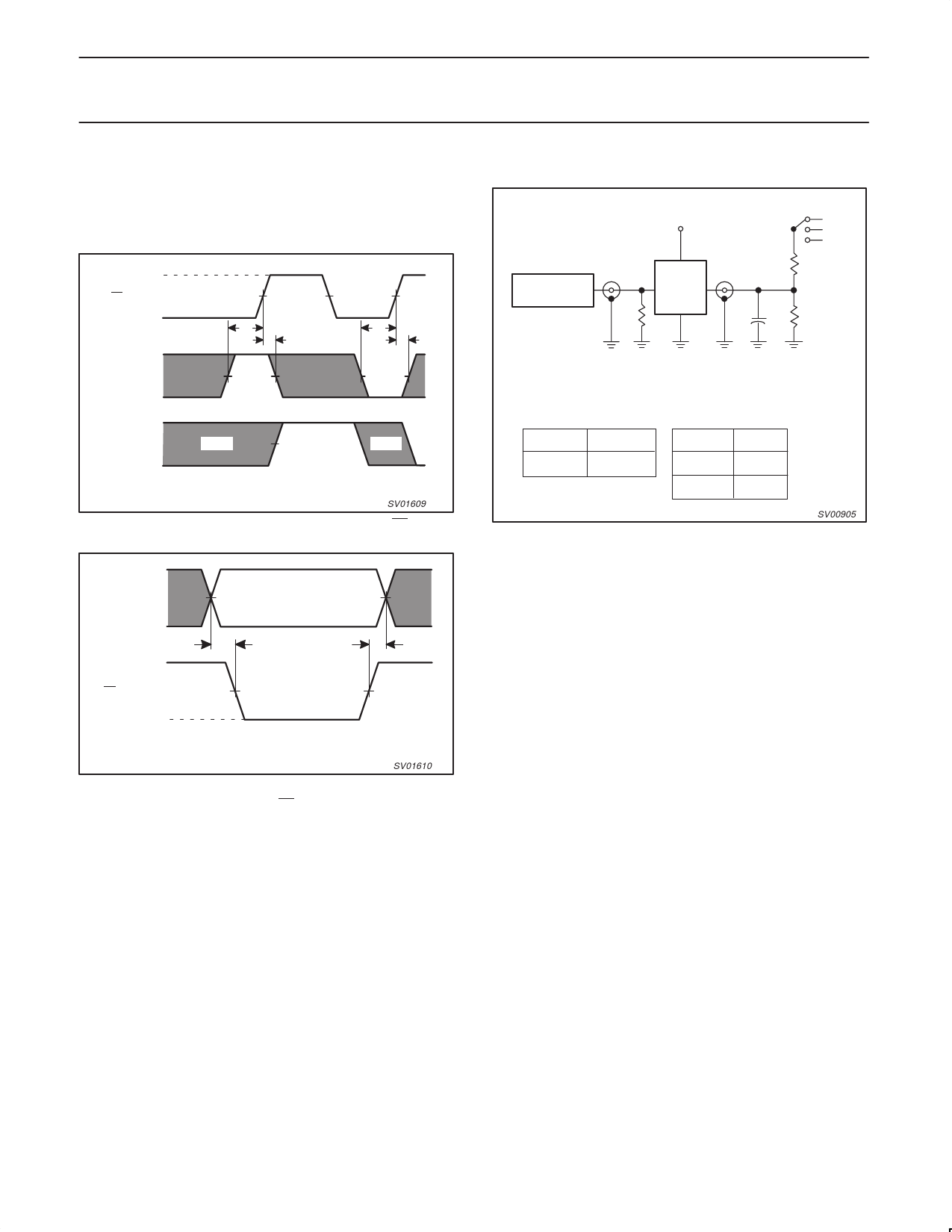
AC WAVEFORMS (Continued)
VM = 1.5 V at VCC ≥ 2.7 V and ≤ 3.6V;
VM = 0.5 × VCC at VCC < 2.7 V and ≥ 4.5 V.
VOL and VOH are the typical output voltage drop that occur with the
output load.
VCC
LE INPUT
GND
VCC
Dn INPUT
GND
VM
tsu
th
VM
tsu
th
VOH
Qn OUTPUT
Q=D
VM
Q=D
VOL
The shaded areas indicate when the input is permitted
to change for predictable output performance
SV01609
Figure 5. Data set-up and hold times for D input to LE input.
VCC
An INPUT
GND
VCC
VM
ADDRESS STABLE
tsu
th
LE INPUT
VM
GND
The shaded areas indicate when the input is permitted to change for predictable
output performance.
SV01610
Figure 6. Address set-up and hold times for
An inputs to LE input.
TEST CIRCUIT
PULSE
GENERATOR
VI
RT
VCC
D.U.T.
S1
2 * VCC
Open
GND
1k
VO
50pF
CL
1k
DEFINITIONS
RL = Load resistor
CL = Load capacitance includes jig and probe capacitance
RT = Termination resistance should be equal to ZOUT of pulse generators.
SWITCH POSITION
TEST
S1
VCC
VI
tPLH/tPHL
Open
< 2.7V
VCC
2.7–3.6V
2.7V
SV00905
Figure 7. Load circuitry for switching times.
1998 May 20
8
Share Link: 