EM19101 Ver la hoja de datos (PDF) - ELAN Microelectronics
Número de pieza
componentes Descripción
Fabricante
EM19101 Datasheet PDF : 6 Pages
| |||
EM19101
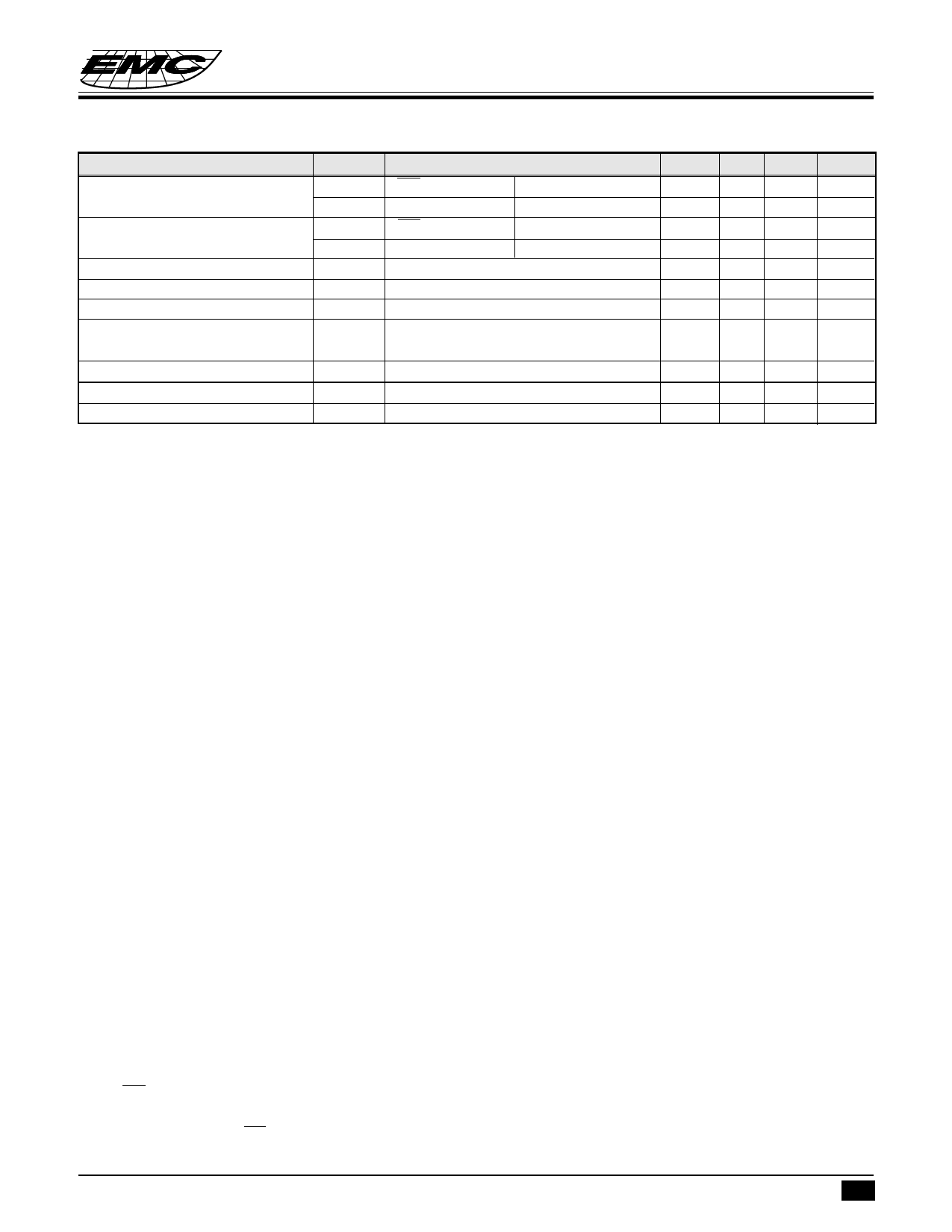
8-BIT 5 MSPS A/D CONVERTER (CMOS)
Parameter
Digital output current
Digital output current
Output data delay
Integral nonlinearity
Differential nonlinearity
Differential gain error
Differential phase error
Aperture jitter
Sampling delay
Sym.
I
OH
IOL
IOZH
TDL
EL
ED
DG
DP
t
AJ
tDS
Conditions
OE=V ,
SS
VDD=min.
OE=VDD,
V =V -0.5V
OH DD
VOL=0.4V
VOH=VDD
V =0V
OL
F =5MSPS V =0.6V to 2.6V
C
IN
FC=5MSPS VIN=0.6V to 2.6V
NTSC 40 IRE mod ramp,
F =14.3MSPS
C
Min. Typ. Max. Unit
-1.1
mA
3.7
16 uA
16
25 40 ns
0.5 1.3 LSB
±0.3 ±0.5 LSB
1.0
%
0.5
°C
30
ps
4
ns
Application Note
VDD,VSS
To reduce noise effects, separate the analog and digital systems close to the device. For both the digital and
analog VDD pins, use a ceramic capacitor of about 0.1uF set as close as possible to the pin to bypass to the
respective GND’s.
Analog input
Compared with the flash type A/D converter, the input capacitance of the analog input is rather small. However
it is necessary to conduct the drive with an amplifier featuring sufficient band and drive capability. When
driving with an amplifier of low output impedance, parasite oscillation may occur. That may be prevented by
inserting a resistance of about 100Ω in series between the amplifier output and A/D input.
Clock input
The clock line wiring should be as short as possible also, to avoid any interference with other signals, separate
it from other circuits
Reference input
Voltage between VRT to VRB is compatible with the dynamic range of the analog input. Bypassing VRT and
V
RB
pins
to
GND,
by
means
of
a
capacitor
about
0.1µF,
stable
characteristics
are
obtained.
By
shorting
V
RT
and VRTS, VRB and VRBS, the self bias function that generates VRT=2.6V and VRB=0.6V, is activated.
Timing
Analog input is sampled with the falling edge of external clock and output as digital data with a delay of 2.5
clocks and with the following rising edge. The delay from the clock rising edge to the data output is about 25ns.
OE pin
By connecting OE to GND output mode is obtained. By connecting to VDD high impedance is obtained.
* This specification are subject to be changed without notice.
4.23.1997 4
Share Link: 