PA3211G-AF5-R(2010) Ver la hoja de datos (PDF) - Unisonic Technologies
Número de pieza
componentes Descripción
Fabricante
PA3211G-AF5-R Datasheet PDF : 5 Pages
| |||
PA3211
Preliminary
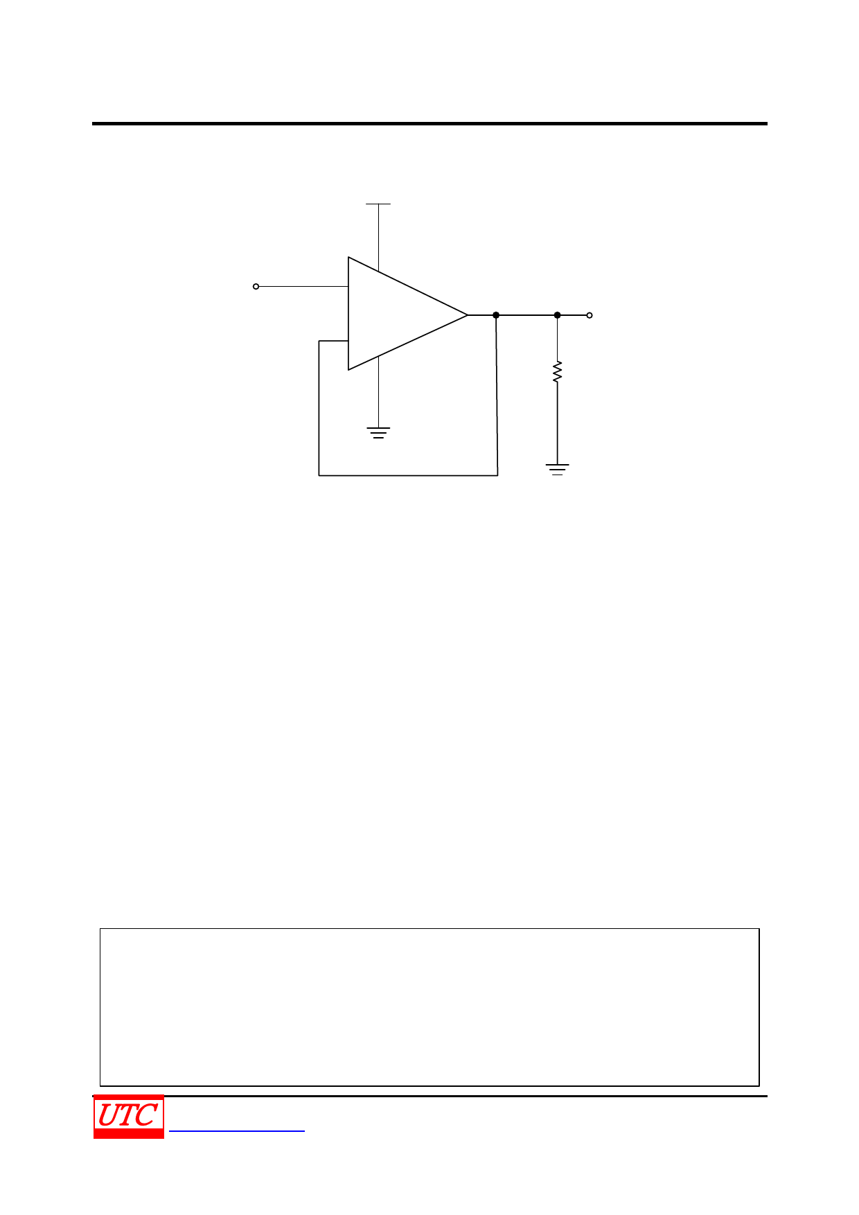
CMOS IC
ABSOLUTE MAXIMUM RATING
PARAMETER
SYMBOL
RATINGS
UNIT
All Other Pins
VSS-0.3 ~ VDD+0.3
V
Supply Voltage
VDD ~ VSS
6.5
V
Power Dissipation (TA=25°C)
PD
520
mW
Junction Temperature
TJ
150
°C
Ambient Operating Temperature
TOPR
-40 ~ +85
°C
Storage Temperature
TSTG
-65 ~ +160
°C
Note: Absolute maximum ratings are those values beyond which the device could be permanently damaged.
Absolute maximum ratings are stress ratings only and functional device operation is not implied.
THERMAL DATA
PARAMETER
Junction to Ambient
SYMBOL
θJA
RATINGS
240
UNIT
°C/W
ELECTRICAL CHARACTERISTICS
(VDD=5V, VSS=0V, TA=25°C, CL=10pF, RL=1kΩ~VDD/2, unless otherwise specified.)
PARAMETER
SYMBOL
TEST CONDITIONS
MIN
Supplies
Supply Voltage Range (Note)
VDD
3
Supply Current
IDD No load
Total Power Dissipation
DC Characteristics
PTOT No load
Input Offset Voltage
VI(OS)
Common Mode Voltage
VCM Inferred from CMRR test
0
Input Bias Current
IB
Input Bias Current Offset
IOS
Input Resistance
RIN
Open Loop Gain
AV
85
Maximum Output Current
Output Voltage Swing High
Output Voltage Swing Low
IO
VOUT=±VINx 90%
VOH RL=2kΩ
VOL RL=2kΩ
55
4.96
Power Supply Rejection Ratio
PSRR 3V≤VDD≤5.5V
45
Common-Mode Rejection Ratio
CMRR VSS≤VCM≤VDD
45
AC Characteristics
Gain-Bandwidth Product
GBWP Open-loop, No load
Slew-Rate
SR Measured from 10%~90% of 4VP-P step,
RL=1kΩ, CL=10pF
Phase Margin
PM
Maximum Output Power
IO
THD<0.1%, RL=16Ω
Notes: Guaranteed by the Power-Supply Rejection Ratio (PSRR) test
TYP MAX
5.5
0.5 0.7
0.25 0.35
±15 ±10
5
±1.5 ±20
±1.5 ±20
1000
95
±66
4.99
0.012 0.04
70
65
6.5
5.23
60
100
UNIT
V
mA
mW
mV
V
nA
nA
MΩ
dB
mA
V
V
dB
dB
MHZ
V/μs
deg
mA
UNISONIC TECHNOLOGIES CO., LTD
www.unisonic.com.tw
4 of 5
QW-R502-451.a
Share Link: 