MT8870 Ver la hoja de datos (PDF) - Mitel Networks
Número de pieza
componentes Descripción
Fabricante
MT8870 Datasheet PDF : 12 Pages
| |||
ISO2-CMOS MT8870D/MT8870D-1
Power-down and Inhibit Mode
A logic high applied to pin 6 (PWDN) will power down
the device to minimize the power consumption in a
standby mode. It stops the oscillator and the
functions of the filters.
Inhibit mode is enabled by a logic high input to the
pin 5 (INH). It inhibits the detection of tones
representing characters A, B, C, and D. The output
code will remain the same as the previous detected
code (see Table 1).
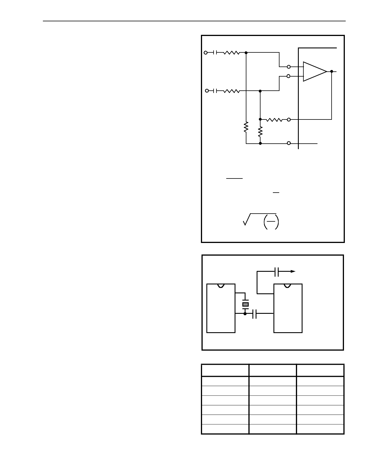
Differential Input Configuration
The input arrangement of the MT8870D/MT8870D-1
provides a differential-input operational amplifier as
well as a bias source (VRef) which is used to bias the
inputs at mid-rail. Provision is made for connection of
a feedback resistor to the op-amp output (GS) for
adjustment of gain. In a single-ended configuration,
the input pins are connected as shown in Figure 10
with the
biasing
op-amp connected for unity
the input at 1/2VDD. Figure
gain and VRef
6 shows the
differential configuration, which permits the
adjustment of gain with the feedback resistor R5.
Crystal Oscillator
The internal clock circuit is completed with the
addition of an external 3.579545 MHz crystal and is
normally connected as shown in Figure 10 (Single-
Ended Input Configuration). However, it is possible
to configure several MT8870D/MT8870D-1 devices
employing only a single oscillator crystal. The
oscillator output of the first device in the chain is
coupled through a 30 pF capacitor to the oscillator
input (OSC1) of the next device. Subsequent devices
are connected in a similar fashion. Refer to Figure 7
for details. The problems associated with
unbalanced loading are not a concern with the
arrangement shown, i.e., precision balancing
capacitors are not required.
C1 R1
MT8870D/
IN+
MT8870D-1
+
-
IN-
C2
R4
R3
R5
GS
R2
VRef
Differential Input Amplifier
C1=C2=10 nF
RR12==6R04k=ΩR,5=R130=037k.Ω5 kΩ
All resistors are ±1% tolerance.
All capacitors are ±5% tolerance.
R3= R2R5
R2+R5
VOLTAGE
GAIN (Av diff)=
R5
R1
INPUT IMPEDANCE
(ZINDIFF) = 2
R12+
1
ωc
2
Figure 6 - Differential Input Configuration
OSC1
X-tal
To OSC1 of next
C
MT8870D/MT8870D-1
OSC2
OSC2
C
OSC1
C=30 pF
X-tal=3.579545 MHz
Figure 7 - Oscillator Connection
Parameter
Unit
Resonator
R1
Ohms
10.752
L1
mH
.432
C1
pF
4.984
C0
pF
37.915
Qm
-
896.37
∆f
%
±0.2%
Table 2. Recommended Resonator Specifications
Note: Qm=quality factor of RLC model, i.e., 1/2ΠƒR1C1.
4-15
Share Link: 