NT7502H-TABF1 Ver la hoja de datos (PDF) - Novatek Microelectronics
Número de pieza
componentes Descripción
Fabricante
NT7502H-TABF1 Datasheet PDF : 54 Pages
| |||
NT7502
System Bus Connection Pads
Pad No.
17 - 24
12
Symbol
D0 - D7
(SI)
(SCL)
A0
I/O
Descriptions
This is an 8-bit bi-directional data bus that connects to an 8-bit or 16-bit
standard MPU data bus.
I/O
When the serial interface is selected (P/S = “L”), then D7 serves as the serial
data input terminal (SI) and D6 serves as the serial clock input terminal (SCL)
At this time, D0 to D5 are set to high impedance.
When the chip select is inactive, D0 to D7 are set to high impedance.
This is connected to the least significant bit of the normal MPU address bus,
and it determines whether the data bits are data or a command
I A0 = “H” indicating that D0 to D7 are display data, and
A0 = “L” indicating that D0 to D7 are control data.
When RES is set to “L”, the settings are initialized.
11
RES
I
The reset operation is performed by the RES signal level.
8, 9
CS1 CS2
I This is the chip select signal. When CS1 = “L” and CS2 = “H”, then the chip
select becomes active, and data/command I/O is enabled.
When connected to an 8080 MPU, it is active LOW.
15
RD
(E)
This pad is connected to the RD signal of the 8080MPU, and the NT7502
I data bus is in an output status when this signal is “L”.
When connected to a 6800 Series MPU, this is active HIGH.
This is used as an enable clock input of the 6800 series MPU.
When connected to an 8080 MPU, this is active LOW. This terminal connects
to the 8080 MPU WR signal. The signals on the data bus are latched at the
14
WR
rising edge of the WR signal.
I When connected to a 6800 Series MPU, this is the read/write control signal
(R/W )
input terminal.
When R / W = “H”: Read
When R / W = “L”: Write
This is the MPU interface switch terminal
75
C86
I C86 = “H”: 6800 Series MPU interface
C86 = “L”: 8080 MPU interface
This is the parallel data input/serial data input switch terminal
P/S = “H”: Parallel data input
P/S = “L”: Serial data input
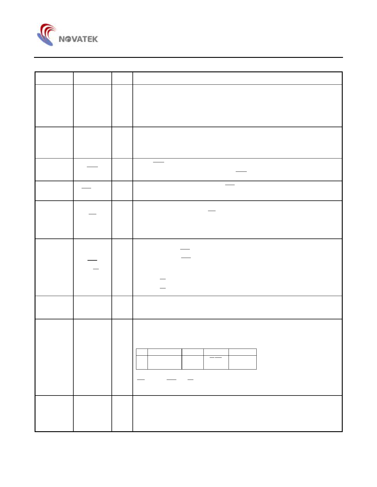
The following applies depending on the P/S status:
P/S Data/Command Data Read/Write Serial Clock
76
P/S
I
"H"
A0
D0 to D7 RDWR
"L"
A0
SI (D7) Write only SCL (D6)
When P/S = “L”, D0 to D5 are HZ. D0 to D5 may be “H”, “L” or Open.
RD (E) and WR ( R / W ) are fixed to either “H” or “L”. With serial data input,
RAM display data reading is not supported.
Terminal is used to select whether enable or disable the display clock internal
oscillator circuit.
73
CLS
I CLS = “H”: Internal oscillator circuit is enabled
CLS = “L”: Internal oscillator circuit is disabled (requires external input).
When CLS = “L”, input the display clock through the CL pad.
6
Share Link: 