P1818F Ver la hoja de datos (PDF) - Alliance Semiconductor
Número de pieza
componentes Descripción
Fabricante
P1818F Datasheet PDF : 8 Pages
| |||
P1818/19/20/21/22
®
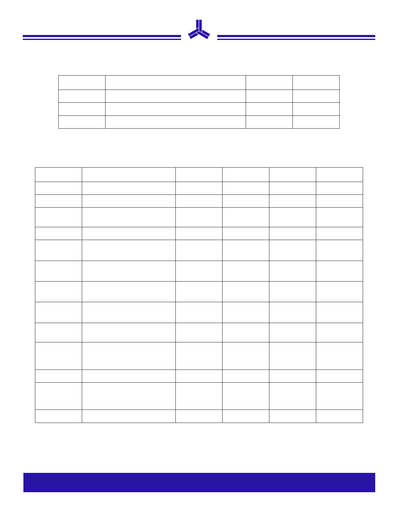
Absolute Maximum Ratings
Symbol
VDD, VIN
TSTG
TA
Parameter
Voltage on any pin with respect to GND
Storage temperature
Operating temperature
DC Electrical Characteristics
3.3 V, 25° C
Symbol
VIL
VIH
IIL
IIH
IXOL
IXOH
VOL
VOH
IDD
ICC
VDD
tON
ZOUT
Parameter
Input low voltage
Input high voltage
Input low current (inputs D_C,
PD#, MRS, FRS, SRS)
Input high current
XOUT output low current
(@ 0.4 V, VDD = 3.3 V)
XOUT output high current
(@ 2.5 V, VDD = 3.3 V)
Output low voltage
(VDD=3.3 V, IOL = 20 mA)
Output high voltage
(VDD=3.3 V, IOH = 20 mA)
Static supply current
Standby mode
Dynamic supply current
Normal mode (3.3 V and 25 pF
probe loading)
Operating voltage
Power up time
(first locked clock cycle after
power up)
Clock output impedance
Min
GND – 0.3
2.00
-60.0
–
2.00
–
–
–
–
7.1
fIN-min
–
–
–
Rating
Unit
-0.5 to +7.0
V
-65 to +125
ºC
0 to +70
ºC
Typ
Max
Unit
–
0.8
V
–
VDD + 0.3
V
–
-20.00
µA
–
1.00
µA
–
12.00
mA
–
12.00
mA
–
0.4
V
–
2.8
V
4.5
–
mA
–
26.9
mA
fIN-max
3.3
–
V
0.18
–
mS
50
–
Ω
March 2003
Low Power Mobile VGA EMI Reduction IC
Notice: The information in this document is subject to change without notice.
5 of 8
Share Link: 