NLSX5014 Ver la hoja de datos (PDF) - ON Semiconductor
Número de pieza
componentes Descripción
Fabricante
NLSX5014 Datasheet PDF : 14 Pages
| |||
NLSX5014
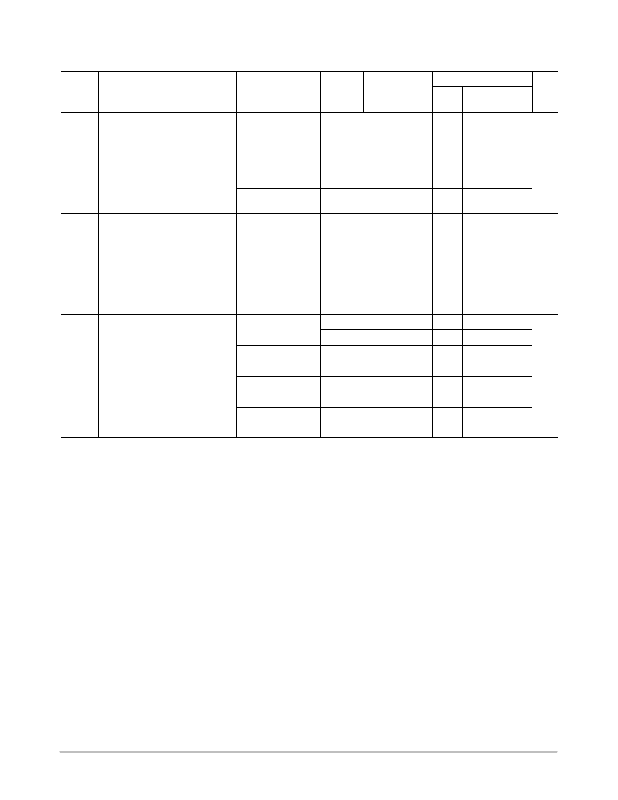
TIMING CHARACTERISTICS (continued)
−555C to +1255C
Symbol
Parameter
Test Conditions
(Note 10)
VCC (V)
(Note 11)
VL (V)
(Note 12)
Typ
Min (Note 13) Max Unit
tEN−VCC I/O_VCC Output Enable Time tPZH
tPZL
tEN−VL I/O_VL Output Enable Time tPZH
tPZL
tDIS−VCC I/O_VCC Output Disable Time tPHZ
tPLZ
tDIS−VL I/O_VL Output Disable Time tPHZ
tPLZ
MDR Maximum Data Rate
CIOVCC = 15 pF,
I/O_VL = VL
CIOVCC = 15 pF,
I/O_VL = 0 V
CIOVL = 15 pF,
I/O_VCC = VCC
CIOVL = 15 pF,
I/O_VCC = 0 V
CIOVCC = 15 pF,
I/O_VL = VL
CIOVCC = 15 pF,
I/O_VL = 0 V
CIOVL = 15 pF,
I/O_VCC = VCC
CIOVL = 15 pF,
I/O_VCC = 0 V
CIO = 15 pF
0.9 – 4.5
0.9 – 4.5
0.9 – 4.5
0.9 – 4.5
0.9 – 4.5
0.9 – 4.5
0.9 – 4.5
0.9 – 4.5
0.9 – 4.5
1.8 – 4.5
0.9 – 4.5
0.9 – 4.5
0.9 – 4.5
0.9 – 4.5
0.9 – 4.5
0.9 – 4.5
0.9 – 4.5
0.9 – 4.5
0.9 – 4.5
1.8 – 4.5
−
−
160 nS
−
−
130
−
−
160 nS
−
−
130
−
−
210 nS
−
−
175
−
−
210 nS
−
−
175
50
−
140
−
− mbps
−
CIO = 30 pF
0.9 – 4.5
0.9 – 4.5
40
−
−
1.8 – 4.5
1.8 – 4.5
120
−
−
CIO = 50 pF
1.0 – 4.5
1.0 – 4.5
30
−
−
1.8 – 4.5
1.8 – 4.5
100
−
−
CIO = 100 pF
1.2 – 4.5
1.2 – 4.5
20
−
−
1.8 – 4.5
1.8 – 4.5
60
−
−
10. Normal test conditions are VI = 0 V, CIOVCC ≤ 15 pF and CIOVL ≤ 15 pF, unless otherwise specified.
11. VCC is the supply voltage associated with the I/O VCC port, and VCC ranges from +0.9 V to 4.5 V under normal operating conditions.
12. VL is the supply voltage associated with the I/O VL port, and VL ranges from +0.9 V to 4.5 V under normal operating conditions.
13. Typical values are for VCC = +2.8 V, VL = +1.8 V and TA = +25°C. All units are production tested at TA = +25°C. Limits over the operating
temperature range are guaranteed by design.
www.onsemi.com
7
Share Link: 