NLSX5014 Ver la hoja de datos (PDF) - ON Semiconductor
Número de pieza
componentes Descripción
Fabricante
NLSX5014 Datasheet PDF : 14 Pages
| |||
NLSX5014
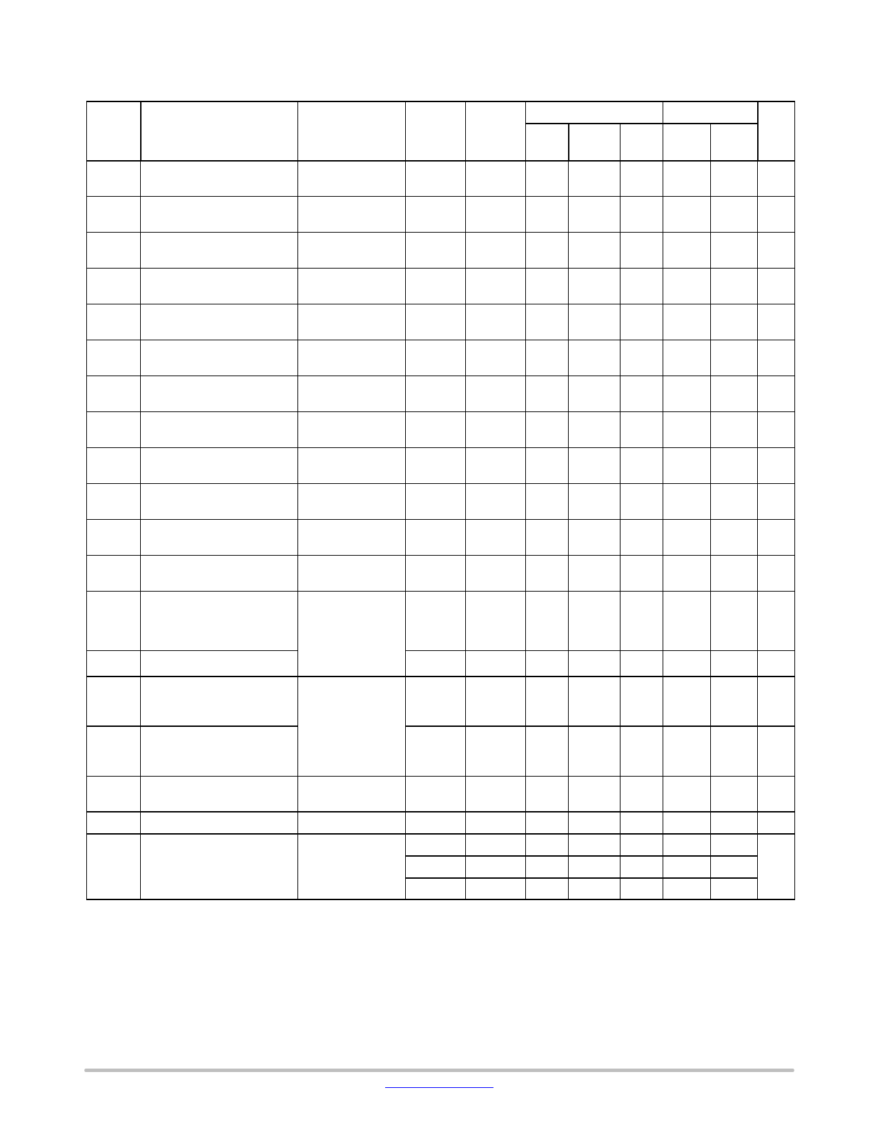
DC ELECTRICAL CHARACTERISTICS
−405C to +855C
−555C to +1255C
Symbol
Parameter
VIHC I/O VCC Input HIGH Voltage
VILC I/O VCC Input LOW Voltage
VIHL I/O VL Input HIGH Voltage
VILL I/O VL Input LOW Voltage
VIH Control Pin Input HIGH Volt-
age
VIL Control Pin Input LOW Volt-
age
VIH Control Pin Input HIGH Volt-
age
Test Conditions
(Note 1)
TA = +25°C
TA = +25°C
TA = +25°C
VCC (V)
(Note 2)
0.9 – 4.5
VL (V)
(Note 3)
0.9 – 4.5
0.9 – 4.5 0.9 – 4.5
0.9 – 4.5 0.9 – 4.5
0.9 – 4.5 0.9 – 4.5
1.2 – 4.5 1.2 – 4.5
1.2 – 4.5 1.2 – 4.5
VCC < 1.2 VL < 1.2
Min
2/3 *
VCC
−
2/3 *
VL
−
2/3 *
VL
−
VL
Typ
(Note 4)
−
−
−
−
−
−
−
Max
−
1/3 *
VCC
−
1/3 *
VL
−
1/3 *
VL
−
Min
2/3 *
VCC
−
2/3 * VL
Max
−
1/3 *
VCC
−
Unit
V
V
V
− 1/3 * VL V
2/3 * VL −
V
− 1/3 * VL V
VL
−
V
VIL Control Pin Input LOW Volt-
TA = +25°C
VCC < 1.2 VL < 1.2
−
−
0
−
0
V
age
VOHC I/O VCC Output HIGH Volt-
I/O VCC source 0.9 – 4.5 0.9 – 4.5 0.9 *
−
age
current = 20 mA
VCC
VOLC I/O VCC Output LOW Voltage
I/O VCC sink
0.9 – 4.5 0.9 – 4.5 −
−
current = 20 mA
−
0.9 *
−
V
VCC
0.2
−
0.2
V
VOHL I/O VL Output HIGH Voltage
I/O VL source
0.9 – 4.5 0.9 – 4.5 0.9 *
−
current = 20 mA
VL
VOLL I/O VL Output LOW Voltage I/O VL sink current 0.9 – 4.5 0.9 – 4.5 −
−
= 20 mA
− 0.9 * VL −
V
0.2
−
0.2
V
IQVCC VCC Supply Current
IQVL VL Supply Current
EN = VL, IO = 0 A, 0.9 – 4.5 0.9 – 4.5 −
(I/O VCC = 0 V or
VCC, I/O VL = float)
or
(I/O VCC = float, I/O
VL = 0 V or VL)
0.9 – 4.5
0.9 – 4.5
−
ITS−VCC VCC Tristate Output Mode
Supply Current
TA = +25°C,
EN = 0 V
0.9 – 4.5 0.9 – 4.5 −
ITS−VL VL Tristate Output Mode
Supply Current
(I/O VCC = 0 V or
VCC, I/O VL = float)
or
0.9 – 4.5 0.9 – 4.5 −
(I/O VCC = float, I/O
VL = 0 V or VL)
IOZ I/O Tristate Output Mode
Leakage Current
TA = +25°C,
EN = 0V
0.9 – 4.5 0.9 – 4.5 −
−
1
−
2.5 mA
−
1
−
2.5 mA
−
0.5
−
1.5 mA
−
0.5
−
1.5 mA
−
±1
−
±1.5 mA
II
Control Pin Input Current
TA = +25°C
0.9 – 4.5 0.9 – 4.5 −
−
±1
−
±1 mA
IOFF Power Off Leakage Current I/O VCC = 0 to 4.5V,
0
0
−
−
1
−
1.5 mA
I/O VL = 0 to 4.5 V 0.9 – 4.5
0
−
−
1
−
1.5
0
0.9 – 4.5 −
−
1
−
1.5
Product parametric performance is indicated in the Electrical Characteristics for the listed test conditions, unless otherwise noted. Product
performance may not be indicated by the Electrical Characteristics if operated under different conditions.
1. Normal test conditions are VI = 0 V, CIOVCC ≤ 15 pF and CIOVL ≤ 15 pF, unless otherwise specified.
2. VCC is the supply voltage associated with the I/O VCC port, and VCC ranges from +0.9 V to 4.5 V under normal operating conditions.
3. VL is the supply voltage associated with the I/O VL port, and VL ranges from +0.9 V to 4.5 V under normal operating conditions.
4. Typical values are for VCC = +2.8 V, VL = +1.8 V and TA = +25°C. All units are production tested at TA = +25°C. Limits over the operating
temperature range are guaranteed by design.
www.onsemi.com
5
Share Link: 