NLAS325USG(2015) Ver la hoja de datos (PDF) - ON Semiconductor
Número de pieza
componentes Descripción
Fabricante
NLAS325USG Datasheet PDF : 10 Pages
| |||
NLAS325
MAXIMUM RATINGS
Symbol
Parameter
Value
Unit
VCC
VI
VO
IIK
IOK
IO
ICC
IGND
TSTG
TL
TJ
qJA
PD
MSL
DC Supply Voltage
DC Input Voltage
DC Output Voltage
DC Input Diode Current
DC Output Diode Current
DC Output Sink Current
DC Supply Current per Supply Pin
DC Ground Current per Ground Pin
Storage Temperature Range
Lead Temperature, 1.0 mm from Case for 10 Seconds
Junction Temperature under Bias
Thermal Resistance (Note 1)
Power Dissipation in Still Air at 85°C
Moisture Sensitivity
VI < GND
VO < GND
*0.5 to )7.0
*0.5 to )7.0
*0.5 to )7.0
*50
*50
$50
$100
$100
*65 to )150
260
)150
250
250
Level 1
V
V
V
mA
mA
mA
mA
mA
°C
°C
°C
°C/W
mW
FR
VESD
Flammability Rating
ESD Withstand Voltage
Oxygen Index: 28 to 34 UL 94 V−0 @ 0.125 in
Human Body Model (Note 2)
> 2000
V
Machine Model (Note 3)
> 200
Charged Device Model (Note 4)
N/A
Stresses exceeding those listed in the Maximum Ratings table may damage the device. If any of these limits are exceeded, device functionality
should not be assumed, damage may occur and reliability may be affected.
1. Measured with minimum pad spacing on an FR4 board, using 10 mm−by−1 inch, 2−ounce copper trace with no air flow.
2. Tested to EIA/JESD22−A114−A.
3. Tested to EIA/JESD22−A115−A.
4. Tested to JESD22−C101−A.
RECOMMENDED OPERATING CONDITIONS
Symbol
Parameter
Min
Max
Unit
VCC
DC Supply Voltage
2.0
5.5
V
VIN
Digital Select Input Voltage
GND
5.5
V
VIS
Analog Input Voltage (NC, NO, COM)
GND
VCC
V
TA
Operating Temperature Range
*55
)125
°C
tr, tf
Input Rise or Fall Time, SELECT
VCC = 3.3 V $ 0.3 V
0
VCC = 5.0 V $ 0.5 V
0
100
ns/V
20
Functional operation above the stresses listed in the Recommended Operating Ranges is not implied. Extended exposure to stresses beyond
the Recommended Operating Ranges limits may affect device reliability.
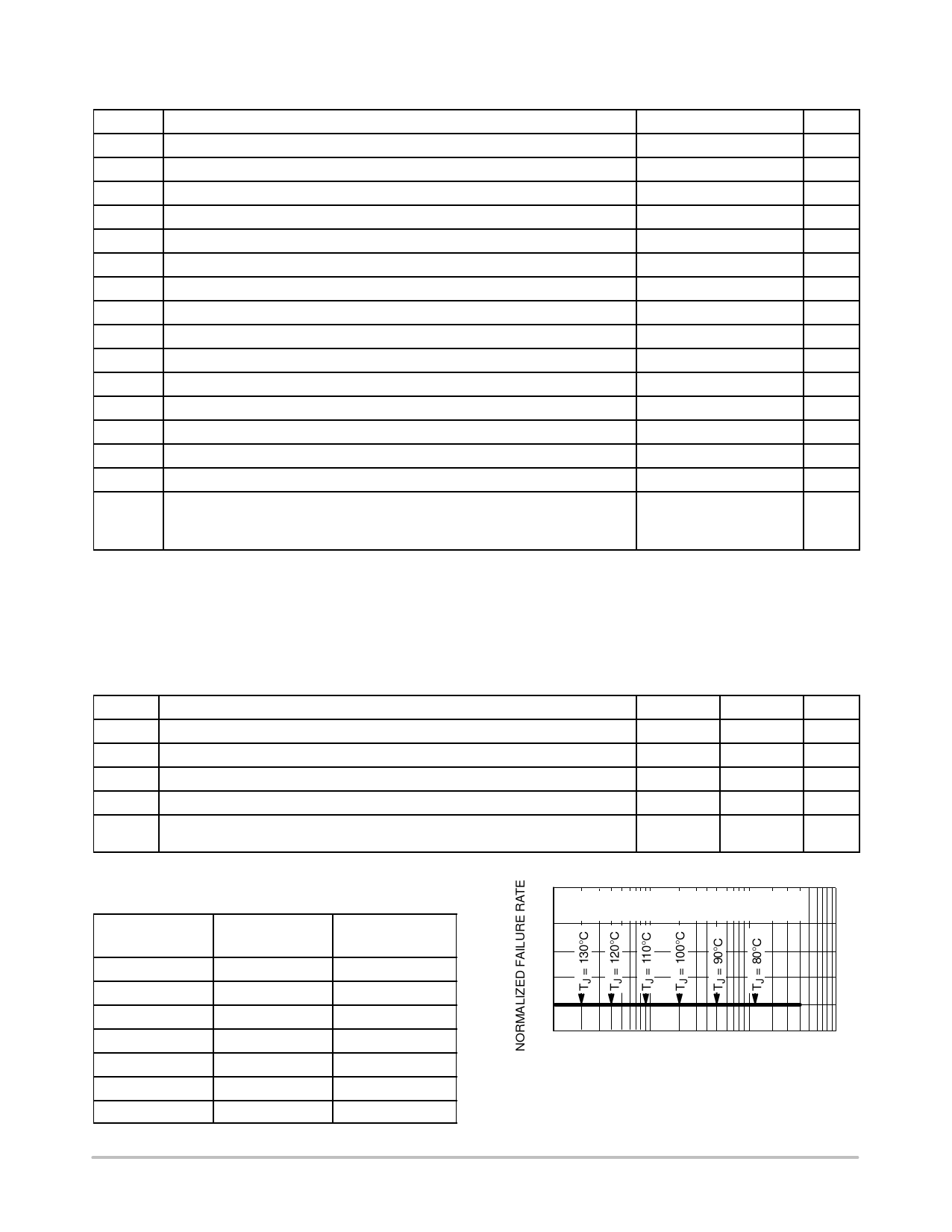
DEVICE JUNCTION TEMPERATURE VERSUS
TIME TO 0.1% BOND FAILURES
Junction
Temperature °C
Time, Hours
Time, Years
FAILURE RATE OF PLASTIC = CERAMIC
UNTIL INTERMETALLICS OCCUR
80
1,032,200
117.8
90
419,300
47.9
1
100
178,700
20.4
110
79,600
9.4
120
37,000
4.2
1
10
100
1000
TIME, YEARS
130
17,800
2.0
140
8,900
1.0
Figure 2. Failure Rate vs. Time Junction Temperature
www.onsemi.com
2
Share Link: 