NJU8753 Ver la hoja de datos (PDF) - Japan Radio Corporation
Número de pieza
componentes Descripción
Fabricante
NJU8753
Japan Radio Corporation

NJU8753 Datasheet PDF : 7 Pages
| |||
NJU3857553
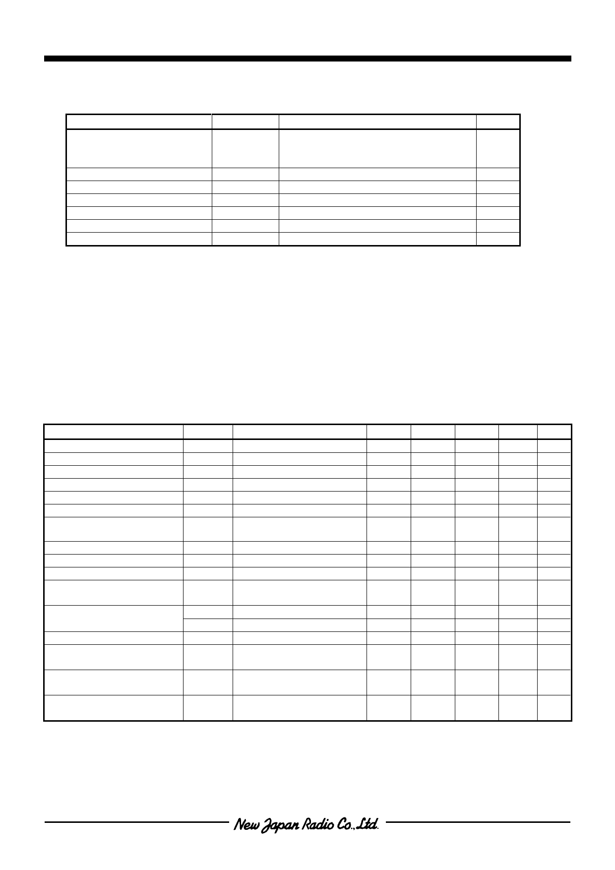
ABSOLUTE MAXIMUM RATINGS
PARAMETER
Supply Voltage
LX Input Voltage
FB Input Voltage
Input Voltage
Operating Temperature
Storage Temperature
Power Dissipation
(Ta=25°C)
SYMBOL
RATING
UNIT
VDD
-0.3 ~ +4.0
V
VREG
-0.3 ~ +4.0
V
VDDO
-0.3 ~ +15.0
V
VLX
-0.3 ~ +15.0
V
VFB
-0.3 ~ +4.0
V
Vin
-0.3 ~ VDD+0.3
V
Topr
-40 ~ +85
°C
Tstg
-40 ~ +125
°C
PD
640*
mW
* : Mounted on a glass epoxy PCB(50mm x 50mm x 1.6mm).
Note 1) All voltage are relative to “VSS= 0V” reference.
Note 2) The LSI must be used inside of the “Absolute maximum ratings”. Otherwise, a stress may cause
permanent damage to the LSI.
Note 3) De-coupling capacitors for VDD(Pin 28)-VSS(Pin 27), VREG(Pin 3)-VSS(Pin 5) and LX(Pin 8,9)-VSS(Pin
17,18,19) should be connected for stable operation.
ELECTRICAL CHARACTERISTIC
(Ta=25°C, VDD=VREG=2.85V, VBAT=3.7V, VDDO=10V, VSS=0V, VSS1=0V,
TEST1=TEST2=TEST3=0V, EN1=EN2=2.85V,
Input Signal=1kHz, Input Signal Level=150mVrms, Frequency Band=20Hz~20kHz,
Load Impedance=2.0µF 2nd-order 11.5kHz LC Filter(Q=0.72))
PARAMETER
SYMBOL
CONDITIONS
MIN TYP MAX UNIT Note
VDD Supply Voltage
VREG Supply Voltage
VBAT Input Voltage
VDDO Supply Voltage
Input Impedance
Voltage Gain
Output THD
Maximum Output
VDD
2.6
VREG
2.6
VBAT
2.6
VDDO
8.0
ZIN
IN pin
-
AV
-
THD
Input Signal Level
=200mVrms
-
Vo Output THD=10%
-
2.85
3.6
V
2.85
3.6
V
3.7
4.2
V
10.0 12.0
V
20
-
KΩ
31
-
dB
0.05 0.08
%
4
8.0
-
Vrms
S/N
SN A weight
-
80
-
dB
4
Operating Current(Standby)
IST
EN1=EN2=0V
Operating Current
(No signal input)
ISS
No-load operating
No Signal Input
-
-
1
µA
-
10
15
mA
Input Voltage
Input Leakage Current
Switching regulator
Oscillating Frequency
VIH EN1, EN2 pins
VIL
EN1, EN2 pins
ILK
EN1, EN2 pins
fOSC
0.7VDD
-
VDD
V
0
-
0.3VDD
V
-
-
±1.0 µA
220
300
380 kHz
Switching regulator
Maximum Load Current
Switching regulator
Load Stability
IOUT
∆VOUT
Step-up Voltage =10.0V
VOUT= 10.0V X 95%
Step-up Voltage =10.0V
IOUT =10mA~50mA
50
-
-
100
-
mA
-
mV
Ver.2003-09-26
-5-
Share Link: