NJU7329A Ver la hoja de datos (PDF) - Japan Radio Corporation
Número de pieza
componentes Descripción
Fabricante
NJU7329A Datasheet PDF : 9 Pages
| |||
NJU7329A
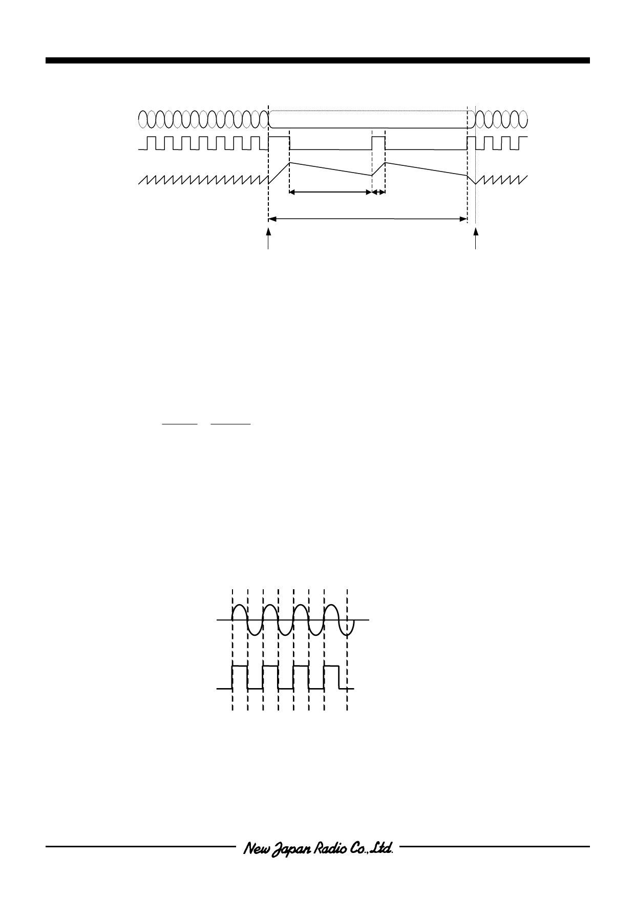
A typical value of C2 is either 0.47uF or 1uF depending on a motor.
Hall input
Motor output
Ct Terminal voltage
Toff
Ton
Motor Lock protection period
Motor Locked
Returns to normal operation
3. Design of hall element bias resistance (R1 and R2)
Hall amplifier is a differential amplifier with hysteresis characteristics (24mV typical).
The common-mode input voltage is between 0.4V and VDD-1V and the input signal must be within the
range.Non-excitation hall bias voltage is to be set at a half of VDD for effective use of common-mode input voltage
range. Therefore the same value of hall bias resistors is selected for R1 and R2.
Given that the bias current is set to be 5mA by HW101A datasheet, R1 and R2 can be determined as follows:
R1+ R2 + Rin
=
VDD
Ihbias
=
5
5 ×10−3
= 1kΩ
R1 = R2 = 300Ω
The output voltage of hall elements is influenced by the bias current and magnetic flux density of hall elements.
The optimum input voltage of NJU7329A is 100mVp-p and higher. With such input voltage, the highest efficiency can
be obtained.
4. Design of FG output resistsnce (R3)
FG Out(FG:Pin8) is a open drain output and R3 is a pull up register. A typical value of R3 is 10kΩ. The timing chart
of FG Out is as follows.
Hall input
IN+
FG Terminal voltage
-8-
Ver.2003-07-28
Share Link: 