NE5550234 Ver la hoja de datos (PDF) - Renesas Electronics
Número de pieza
componentes Descripción
Fabricante
NE5550234 Datasheet PDF : 16 Pages
| |||
NE5550234
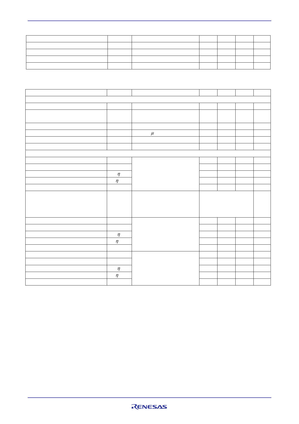
RECOMMENDED OPERATING RANGE (TA = 25°C)
Parameter
Drain to Source Voltage
Gate to Source Voltage
Drain Current
Input Power
Symbol
VDS
VGS
IDS
Pin
Test Conditions
f = 460 MHz, VDS = 7.5 V
MIN.
−
1.65
−
−
TYP.
7.5
2.20
0.38
15
MAX.
9.0
2.85
−
20
Unit
V
V
A
dBm
ELECTRICAL CHARACTERISTICS (TA = 25°C, unless otherwise specified)
Parameter
Symbol
Test Conditions
MIN. TYP. MAX.
DC Characteristics
Gate to Source Leakage Current
Drain to Source Leakage Current
(Zero Gate Voltage Drain Current)
IGSS
VGS = 6.0 V
IDSS
VDS = 25 V
−
−
100
−
−
10
Gate Threshold Voltage
Drain to Source Breakdown Voltage
Transconductance
Thermal Resistance
Vth
BVDSS
Gm
Rth
VDS = 7.5 V, IDS = 1.0 mA
IDS = 10 μA
VDS = 7.5 V, IDS = 140±20 mA
Channel to Case
1.15 1.65 2.25
25
38
−
−
0.44
−
−
10.0
−
RF Characteristics
Output Power
Drain Current
Power Drain Efficiency
Power Added Efficiency
Linear Gain
Load VSWR Tolerance
Pout
IDS
ηd
ηadd
GL Note 1
Note 2
f = 460 MHz, VDS = 7.5 V,
Pin = 15 dBm,
IDset = 40 mA (RF OFF)
f = 460 MHz, VDS = 9.0 V,
Pin = 15 dBm,
IDset = 40 mA (RF OFF)
Load VSWR=20:1(All Phase)
31.5 33.0
−
−
0.38
−
−
70
−
−
68
−
−
23.5
−
No Destroy
Output Power
Drain Current
Power Drain Efficiency
Power Added Efficiency
Linear Gain
Output Power
Drain Current
Power Drain Efficiency
Power Added Efficiency
Linear Gain
Pout
IDS
ηd
ηadd
GL Note 3
Pout
IDS
ηd
ηadd
GL Note 4
f = 157 MHz, VDS = 7.5 V,
Pin = 15 dBm,
IDset = 40 mA (RF OFF)
f = 900 MHz, VDS = 7.5 V,
Pin = 17 dBm,
IDset = 40 mA (RF OFF)
−
33.0
−
−
0.36
−
−
74
−
−
73
−
−
25.8
−
−
32.2
−
−
0.35
−
−
62
−
−
60
−
−
18.3
−
Notes: 1. Pin = 0 dBm
2. These characteristics values are measurement using measurement tools especially by RENESAS.
3. Pin = −5 dBm
4. Pin = 7 dBm
Unit
nA
μA
V
V
S
°C/W
dBm
A
%
%
dB
dBm
A
%
%
dB
dBm
A
%
%
dB
Remark DC performance is 100% testing. RF performance is testing several samples per wafer.
The wafer rejection criterion for standard devices is 1 reject for several samples.
R09DS0039EJ0300 Rev.3.00
Mar 12, 2013
Page 2 of 14
Share Link: 