SPT7830SCS Ver la hoja de datos (PDF) - Signal Processing Technologies
Número de pieza
componentes Descripción
Fabricante
SPT7830SCS Datasheet PDF : 8 Pages
| |||
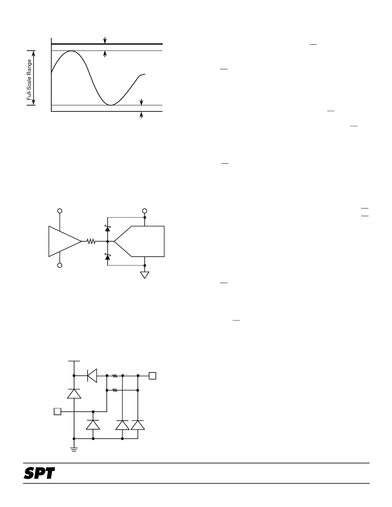
Figure 1 - Analog Input Full-Scale Range
VREF+
+FS
6% of [(VREF+) - (VREF-)]
-FS
VREF-
4% of [(VREF+) - (VREF-)]
The drive requirements for the analog input are minimal when
compared to most other converters due to the SPT7830’s
extremely low input capacitance of only 5 pF and very high
input resistance of greater than 5 MΩ.
If the input buffer amplifier supply voltages are greater than
VDD + 0.7 V or less than Ground - 0.7 V, the analog input
should be protected through a series resistor and a diode
clamping circuit as shown in figure 2.
Figure 2 - Recommended Input Protection Circuit
+V
AVDD
Buffer
D1
47 Ω
D2
ADC
-V
D1 = D2 = Hewlett Packard HP5712 or equivalent
INPUT PROTECTION
All I/O pads are protected with an on-chip protection circuit
shown in figure 3. This circuit provides ESD robustness to
>3.0 kV and prevents latch-up under severe discharge con-
ditions without degrading analog transition times.
Figure 3 - On-Chip Protection Circuit
VDD
120 Ω
Analog
MODES OF OPERATION
The SPT7830 has three modes of operation.The mode of
operation is based strictly on how the SC is used.
SINGLE SHOT MODE
When SC goes low, conversion starts on the next rising edge
of the clock (defined as the first conversion clock). The MSB
of data is valid 8 ns after the falling edge of the fourth
conversion clock. (See figure 8, Data Output Timing.)
The conversion is complete after 14 clock cycles. At the
falling edge of the fourteenth clock cycle, if SC is high (not
selected), the data output goes to a high impedance state,
and no more conversions will take place until the next SC low
event. (See the single shot mode timing diagram in figure 4.)
SYNCHRONIZED MODE
When SC goes low, conversion will start on the next rising
edge of the clock (defined as the first conversion clock). The
MSB is valid 8 ns after the falling edge of the fourth conversion
clock.
The first conversion is complete after 14 clock cycles. At any
time after the falling edge of the fourteenth clock cycle, SC
may go low again to initiate the next conversion. When the SC
goes low, the conversion starts on the rising edge of the next
clock. (See the synchronized mode timing diagram in figure 5.)
The data output will go to a high impedance state until the next
conversion is initiated.
FREE RUN MODE
When SC goes low, conversion starts on the next rising edge
of the clock (defined as the first conversion clock). The MSB
data is valid 8 ns after the falling edge of the fourth conversion
clock.
As long as SC is held low, the device operates in the free run
mode. New conversions start after every fourteenth cycle
with valid data available 8 ns after the falling edge of the fourth
clock within each new conversion cycle.
The data output remains low between conversion cycles.
(See the free run mode timing diagram in figure 6.)
120 Ω
Pad
SPT
5
SPT7830
12/19/97
Share Link: 