NCV8667(2010) Ver la hoja de datos (PDF) - ON Semiconductor
Número de pieza
componentes Descripción
Fabricante
NCV8667 Datasheet PDF : 15 Pages
| |||
NCV8667
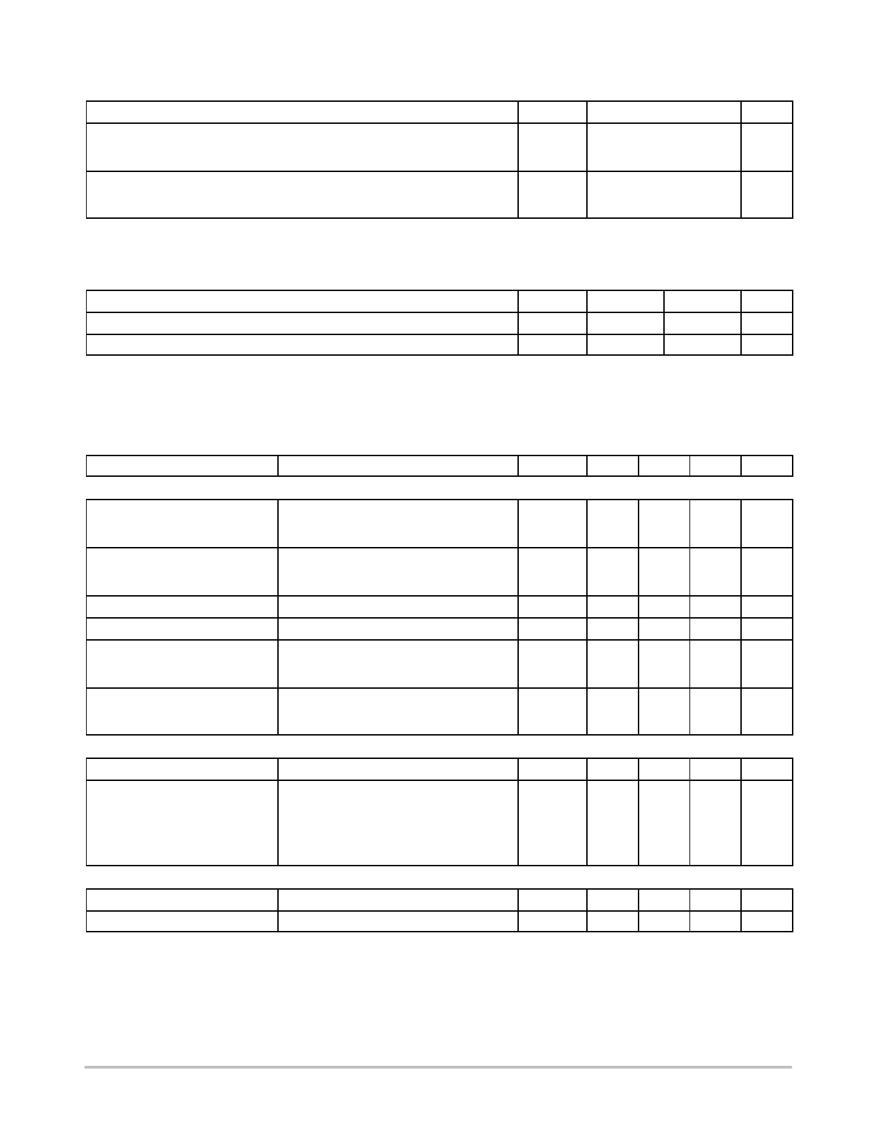
ELECTRICAL CHARACTERISTICS Vin = 13.2 V, VEN = 3 V, VDT = GND, VSI = Vout, RSI1 & RSI2 not used, Cin = 0.1 mF, Cout =
2.2 mF, for typical values TJ = 25°C, for min/max values TJ = −40 °C to 150°C; unless otherwise noted. (Notes 9 and 10)
Parameter
Test Conditions
Symbol
Min
Typ
Max
Unit
ENABLE
Enable Input Threshold Voltage
Logic Low
Logic High
Vth(EN)
−
V
−
0.8
2.5
−
−
Enable Input Current
Logic High VEN = 5 V
Logic Low VEN = 0 V, TJ < 85 °C
DT (Reset Delay Time Select)
μA
IEN_ON
−
3
5
IEN_OFF
−
0.5
1
DT Threshold Voltage
Logic Low
Logic High
Vth(DT)
−
2
V
−
0.8
−
−
DT Input Current
RESET OUTPUT RO
VDT = 5 V
IDT
−
−
1
μA
Output Voltage Reset Threshold
(Note 13)
Reset Hysteresis
Maximum Reset Sink Current
Reset Output Low Voltage
Reset Output High Voltage
Integrated Reset Pull Up Resistor
Reset Delay Time (Note 13)
Reset Reaction Time (see Figure
29)
Vout decreasing
Vin > 5.5 V
Vout = 4.5 V, VRO = 0.25 V
Vout > 1 V, IRO < 200 mA
DT connected to GND
DT connected to Vout
VRT
VRH
IROmax
VROL
VROH
RRO
tRD
tRR
90
−
1.75
−
4.5
15
6.4
102.4
16
93
2.0
−
0.15
−
30
8
128
25
96
−
−
0.25
−
50
9.6
153.6
38
%Vout
%Vout
mA
V
V
kW
ms
μs
EARLY WARNING (SI and SO)
Sense Input Threshold
(NCV8667y0)
High
Low
VSI(th)
V
1.25 1.33 1.40
1.20 1.25 1.33
Sense Input Current (NCV8667y0)
Integrated Sense Output Pull Up
Resistor
VSI = 5 V
ISI
−1
0.1
1
μA
RSO
15
30
50
kW
Sense Output Low Voltage
Sense Output High Voltage
Maximum Sense Output Sink
Current
SI High to SO High Reaction Time
SI Low to SO Low Reaction Time
THERMAL SHUTDOWN
VSI < 1.2 V, ISO < 200 mA, Vout > 1 V
Vout = 4.5 V, VSI < 1.2 V, VSO = 0.25 V
VSI increasing
VSI decreasing
VSOL
−
0.15 0.25
V
VSOH
4.5
−
−
V
ISOmax
1.75
−
mA
−
tPSOLH
tPSOHL
−
7
12
μs
−
3.8
5.0
μs
Thermal Shutdown Temperature
(Note 12)
TSD
150
175
195
°C
Thermal Shutdown Hysteresis
(Note 12)
TSH
−
25
−
°C
9. Refer to ABSOLUTE MAXIMUM RATINGS and APPLICATION INFORMATION for Safe Operating Area.
10. Performance guaranteed over the indicated operating temperature range by design and/or characterization tested at TA [TJ. Low duty
cycle pulse techniques are used during testing to maintain the junction temperature as close to ambient as possible.
11. Measured when output voltage falls 100 mV below the regulated voltage at Vin = 13.2 V.
12. Values based on design and/or characterization.
13. See APPLICATION INFORMATION section for Reset Thresholds and Reset Delay Time Options.
http://onsemi.com
6
Share Link: 