NCV4299 Ver la hoja de datos (PDF) - ON Semiconductor
Número de pieza
componentes Descripción
Fabricante
NCV4299 Datasheet PDF : 23 Pages
| |||
I
INH
SI
RADJ
Bandgap
Reference
−
+
NCV4299
Current Limit and
Saturation Sense
Q
RSO
RRO
SO
1.36 V
+
−
RO
8 mA
+
+
−
−
+
1.85 V
D
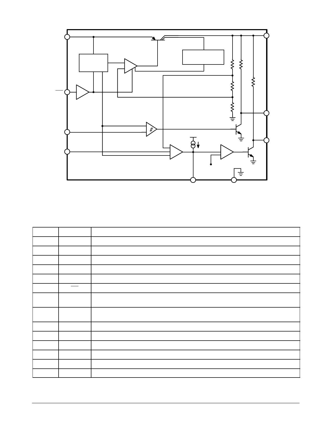
Figure 2. SO−14 Simplified Block Diagram
GND
PIN FUNCTION DESCRIPTION − SO−14 PACKAGE
Pin
Symbol
Description
1
RADJ
Reset Adjust. Use resistor divider to Q to adjust reset threshold lower. Connect to GND if not used.
2
D
Reset Delay. Connect external capacitor to ground to set delay time.
3
GND
Ground.
4
GND
Ground.
5
GND
Ground.
6
INH
Inhibit. Connect to I if not needed. A high turns the regulator on.
7
RO
Reset Output. NPN collector output with internal 20 kW pullup to Q. Notifies user of out of regulation condi-
tion.
8
SO
Sense Output. NPN collector output with internal 20 kW pullup to Q. Can be used to provide early warning
of an impending reset condition.
9
Q
5.0 V, 3.3 V, "2%, 150 mA output. Use 22 mF, ESR t 5.0 W to ground.
10
GND
Ground.
11
GND
Ground.
12
GND
Ground.
13
I
Input. Battery Supply Input Voltage.
14
SI
Sense Input. Can provide an early warning signal of an impending reset condition when used with SO.
http://onsemi.com
3
Share Link: 