NCP629 Ver la hoja de datos (PDF) - ON Semiconductor
Número de pieza
componentes Descripción
Fabricante
NCP629 Datasheet PDF : 11 Pages
| |||
NCP629
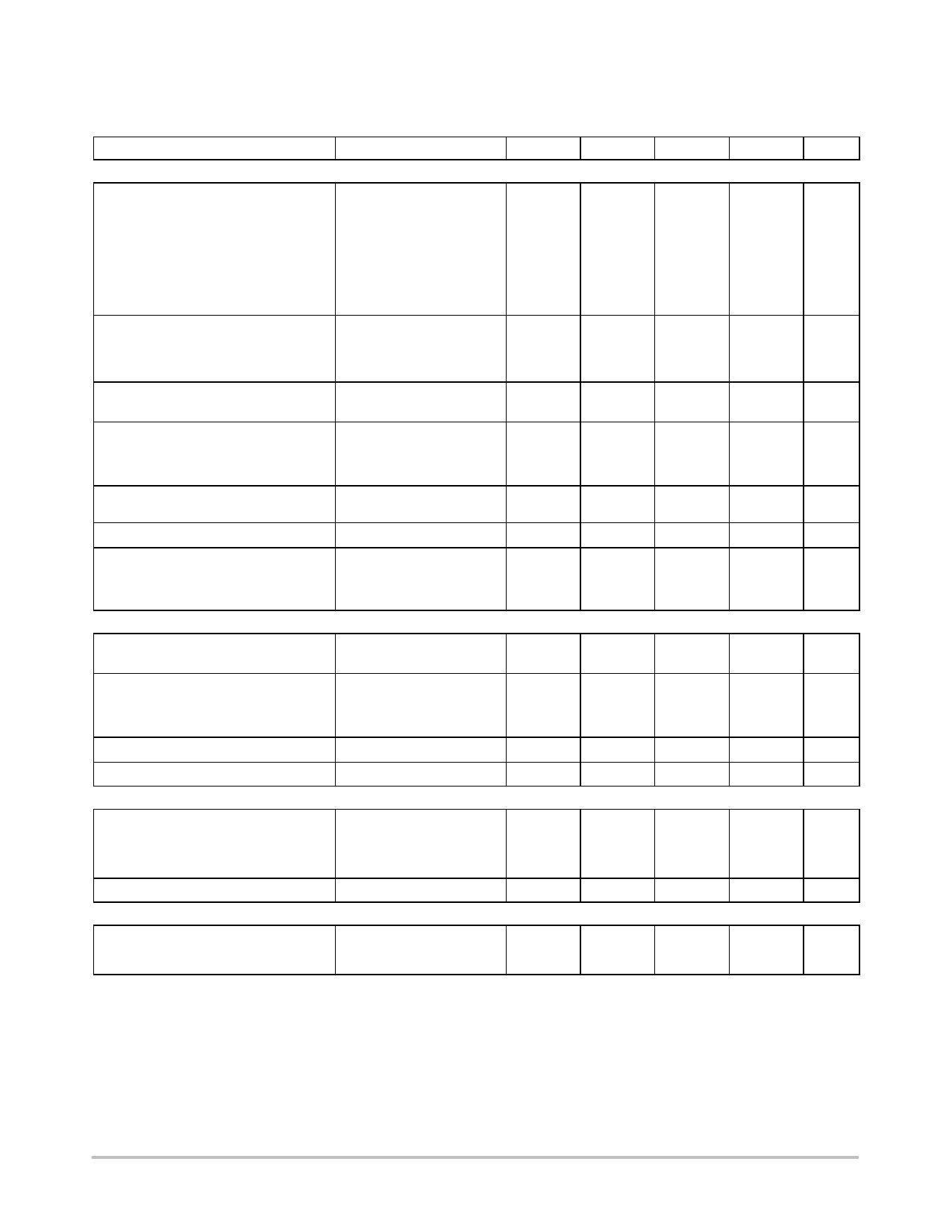
ELECTRICAL CHARACTERISTICS
(Vin = Vout + 0.5 V, Cin = Cout =1.0 mF, for typical values TA = 25°C, for min/max values TA = -40°C to 125°C; unless otherwise noted.)
(Note 7)
Parameter
Test Conditions
Symbol
Min
Typ
Max
Unit
Regulator Output
Output Voltage
1.5 V
1.8 V
2.8 V
3.0 V
3.3 V
3.5 V
5.0 V
Iout = 1.0 mA to 150 mA
Vin = (Vout + 0.5 V) to 6.0 V
Vout
1.470
1.764
2.744
2.940
3.234
3.430
4.900
(-2%)
V
1.530
1.836
2.856
3.060
3.366
3.570
5.100
(+2%)
Power Supply Ripple Rejection (Note 8) Iout = 1.0 mA to 150 mA
PSRR
dB
(Vin = Vout + 1.0 V + 0.5 Vp-p)
f = 120 Hz
-
62
-
f = 1.0 kHz
-
55
-
f = 10 kHz
-
38
-
Line Regulation
Vin = (Vout + 0.5 V) to 6.0 V, Regline
-
Iout = 1.0 mA
1.0
10
mV
Load Regulation
1.5 V
1.8 V
2.8 V to 5.0 V
Iout = 1.0 mA to 150 mA
Regload
-
-
-
mV
2.0
20
2.0
25
2.0
30
Output Noise Voltage (Note 8)
Vout = 1.5 V,
f = 10 Hz to 100 kHz
Vn
-
50
-
mVrms
Output Short Circuit Current
Dropout Voltage
1.5 V
1.8 V
2.8 V to 5.0 V
Vout = 0 V
Isc
300
550
800
mA
Measured at: Vout – 2.0%
VDO
mV
Iout = 150 mA
-
150
225
-
125
175
-
75
125
General
Disable Current
Ground Current
1.5 V
1.8 V to 3.0 V
3.3 V to 5.0 V
ENABLE = 0 V, Vin = 6 V
IDIS
-
-40°C ≤ TA ≤ 85°C
ENABLE = 0.9 V,
IGND
Iout = 1.0 mA to 150 mA
-
-
-
0.01
1.0
mA
mA
135
170
140
175
145
180
Thermal Shutdown Temperature (Note 8)
Thermal Shutdown Hysteresis (Note 8)
TSD
-
175
-
°C
TSH
-
10
-
°C
Chip Enable
ENABLE Input Threshold Voltage
Voltage Increasing, Logic High
Vth(EN)
0.9
-
V
-
Voltage Decreasing, Logic Low
-
-
0.4
Enable Input Bias Current (Note 8)
IEN
-
3.0
100
nA
Timing
Output Turn On Time
1.5 V to 3.5 V
5.0 V
ENABLE = 0 V to Vin
ton
ms
-
15
25
-
30
50
7. Performance guaranteed over the indicated operating temperature range by design and/or characterization, production tested at
TJ = TA = 25 °C. Low duty cycle pulse techniques are used during testing to maintain the junction temperature as close to ambient as possible.
8. Values based on design and/or characterization.
http://onsemi.com
3
Share Link: 