NCP3020A Ver la hoja de datos (PDF) - ON Semiconductor
Número de pieza
componentes Descripción
Fabricante
NCP3020A Datasheet PDF : 23 Pages
| |||
NCP3020A, NCP3020B, NCV3020A, NCV3020B
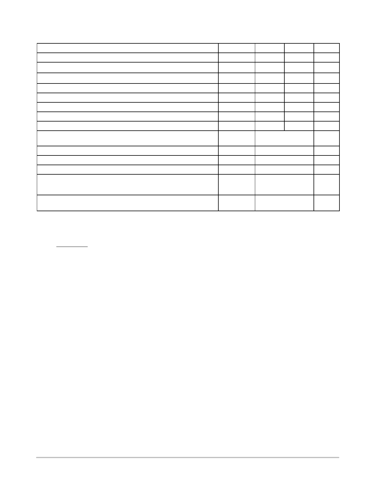
ABSOLUTE MAXIMUM RATINGS (measured vs. GND pin 8, unless otherwise noted)
High Side Drive Boost Pin
Rating
Symbol
BST
VMAX
45
VMIN
−0.3
Unit
V
Boost to VSW differential voltage
BST−VSW
13.2
−0.3
V
COMP
COMP
5.5
−0.3
V
Feedback
High−Side Driver Output
Low−Side Driver Output
Main Supply Voltage Input
Switch Node Voltage
Maximum Average Current
VCC, BST, HSDRV, LSDRV, VSW, GND
Operating Junction Temperature Range (Note 1)
Maximum Junction Temperature
Storage Temperature Range
Thermal Characteristics (Note 2)
SOIC−8 Plastic Package
Thermal Resistance Junction−to−Air
Lead Temperature Soldering (10 sec): Reflow (SMD styles only) Pb−Free
(Note 3)
FB
HSDR
LSDR
VCC
VSW
Imax
TJ
TJ(MAX)
Tstg
RqJA
RF
5.5
−0.3
V
40
−0.3
V
13.2
−0.3
V
40
−0.3
V
40
−0.6
V
mA
130
−40 to +140
°C
+150
°C
−55 to +150
°C
165
260 Peak
°C/W
°C
Stresses exceeding Maximum Ratings may damage the device. Maximum Ratings are stress ratings only. Functional operation above the
Recommended Operating Conditions is not implied. Extended exposure to stresses above the Recommended Operating Conditions may affect
device reliability.
1. The maximum package power dissipation limit must not be exceeded.
TJ(max) * TA
PD +
RqJA
2. When mounted on minimum recommended FR−4 or G−10 board
3. 60−180 seconds minimum above 237°C.
http://onsemi.com
3
Share Link: 