NCP3020A Ver la hoja de datos (PDF) - ON Semiconductor
Número de pieza
componentes Descripción
Fabricante
NCP3020A Datasheet PDF : 23 Pages
| |||
NCP3020A, NCP3020B, NCV3020A, NCV3020B
VCC
INTERNAL BIAS
POR/STARTUP
THERMAL SD
VC
BOOST
CLAMP
COMP
FB
OSCILLATOR
CLK/
DMAX/
SOFT
START
RAMP
1.5 V
GATE
DRIVE
LOGIC
REF
OTA
+
−
PWM
COMP
LEVEL
SHIFT
VCC
CURRENT SAMPLE &
LIMIT
HOLD
ISET
VC
+
−
OOV
OUV
+
−
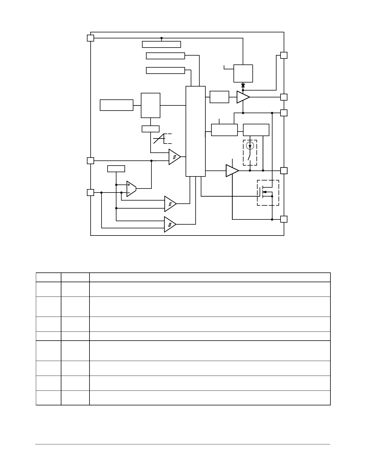
Figure 2. NCP3020 Block Diagram
BST_CHRG
BST
HSDR
VSW
LSDR
GND
PIN FUNCTION DESCRIPTION
Pin Pin Name
Description
1
VCC
The VCC pin is the main voltage supply input. It is also used in conjunction with the VSW pin to sense current
in the high side MOSFET.
2
COMP The COMP pin connects to the output of the Operational Transconductance Amplifier (OTA) and the positive
terminal of the PWM comparator. This pin is used in conjunction with the FB pin to compensate the voltage
mode control feedback loop.
3
FB
The FB pin is connected to the inverting input of the OTA. This pin is used in conjunction with the COMP pin to
compensate the voltage mode control feedback loop.
4
GND
Ground Pin
5
LSDR The LSDR pin is connected to the output of the low side driver which connects to the gate of the low side
N−FET. It is also used to set the threshold of the current limit circuit (ISET) by connecting a resistor from LSDR
to GND.
6
VSW
The VSW pin is the return path for the high side driver. It is also used in conjunction with the VCC pin to sense
current in the high side MOSFET.
7
HSDR The HSDR pin is connected to the output of the high side driver which connects to the gate of the high side
N−FET.
8
BST
The BST pin is the supply rail for the gate drivers. A capacitor must be connected between this pin and the
VSW pin.
http://onsemi.com
2
Share Link: 