NCP1417(2002) Ver la hoja de datos (PDF) - ON Semiconductor
Número de pieza
componentes Descripción
Fabricante
NCP1417 Datasheet PDF : 16 Pages
| |||
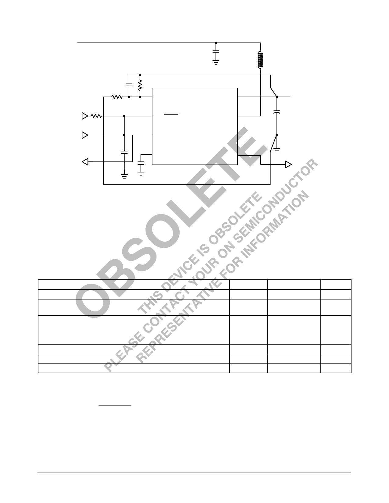
Input
1.0 V to
VOUT
Low Battery
Sense Input
Shutdown
Input
Low Battery
Open Drain
Output 1
NCP1417
10 mF
150 pF
200 K
56 nF
355 K
FB
VOUT
LBI/SHDN
NCP1417
LBO1
LX
GND
REF
150 nF
LBO2
Figure 1. Typical Operating Circuit
22 mH
+ VOUT
33 mF
Output 1.5 V to 5.5 V
IOUT typical up to
200 mA at 3.3 V Output
and 2.5 V Input
Low Battery
Open Drain
Output 2
MAXIMUM RATINGS
Rating
Power Supply (Pin 8)
Input/Output Pins
Pin 1–5, Pin 7
Thermal Characteristics
Micro8 Plastic Package
Maximum Power Dissipation @ TA = 25°C
Thermal Resistance Junction to Air
Operating Junction Temperature Range
Operating Ambient Temperature Range
Storage Temperature Range
1. This device contains ESD protection and exceeds the following tests:
Human Body Model (HBM) "2.0 kV per JEDEC standard: JESD22–A114.
Machine Model (MM) "200 V per JEDEC standard: JESD22–A115.
2. The maximum package power dissipation limit must not be exceeded.
PD
+
TJ(max) *
RqJA
TA
3. Latch–up Current Maximum Rating: "150 mA per JEDEC standard: JESD78.
4. Moisture Sensitivity Level: MSL 1 per IPC/JEDEC standard: J–STD–020A.
Symbol
VOUT
VIO
PD
RqJA
TJ
TA
Tstg
Value
Unit
–0.3 to 6.0
V
–0.3 to 6.0
V
520
240
–40 to +150
–40 to +85
–55 to +150
mW
_C/W
_C
_C
_C
http://onsemi.com
2
Share Link: 