NCP1034(2008) Ver la hoja de datos (PDF) - ON Semiconductor
Número de pieza
componentes Descripción
Fabricante
NCP1034 Datasheet PDF : 23 Pages
| |||
NCP1034
100V Synchronous PWM
Buck Controller
Description
The NCP1034 is a high voltage PWM controller designed for high
performance synchronous Buck DC/DC applications with input
voltages up to 100 V. The NCP1034 drives a pair of external
N−MOSFETs. The switching frequency is programmable from
25 kHz up to 500 kHz allowing the flexibility to tune for efficiency
and size. A synchronization feature allows the switching frequency to
be set by an external source or output a synchronization signal to
multiple NCP1034 controllers. The output voltage can be precisely
regulated using the internally trimmed 1.25 V reference voltage for
low voltage applications. Protection features include user
programmable undervoltage lockout and hiccup current limit.
Features
• High Voltage Operating up to 100 V
• Programmable Switching Frequency up to 500 kHz
• 2 A Output Drive Capability
• Precision Reference Voltage (1.25 V)
• Programmable Soft−Start with Prebiased Load Capability
• Programmable Overcurrent Protection
• Programmable Undervoltage Protection
• Hiccup Current Limit Using MOSFET RDS(on) Sensing
• External Frequency Synchronization
• 16 Pin SOIC Package
• This is a Pb−Free Device
Applications
• 48 V Non−Isolated DC−DC Converter
• Embedded Telecom Systems
• Networking and Computing Voltage Regulator
• Distributed Point of Load Power Architectures
• General High Voltage DC−DC Converters
http://onsemi.com
SOIC−16
D SUFFIX
CASE 751B
A
= Assembly Location
WL = Wafer Lot
Y
= Year
WW = Work Week
G
= Pb−Free Package
MARKING
DIAGRAM
NCP1034D
AWLYWWG
PIN CONNECTIONS
OCset 1
FB 2
Comp 3
SS/SD 4
SYNC 5
PGND 6
16 UVLO
15 RT
14 GND
13 OCIN
12 VCC
11 VS
LDRV 7
DRVCC 8
10 HDRV
9 VB
(Top View)
ORDERING INFORMATION
See detailed ordering and shipping information in the package
dimensions section on page 22 of this data sheet.
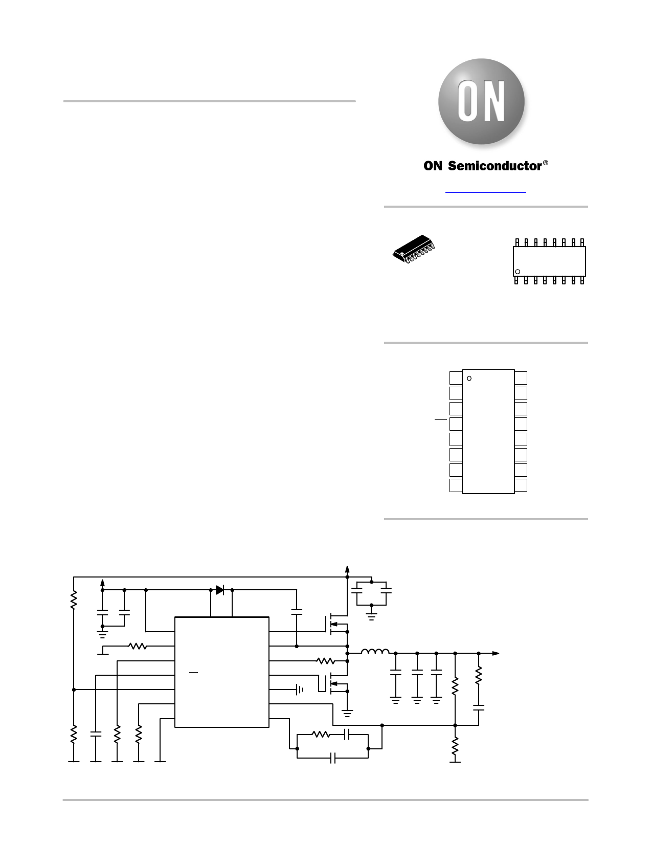
R4
110k
VCC: 12 V
C2 C3
100n 100n
GND GND R10
10k
GND
D1
1N4148
8
9
12 VCC DRVVCC VB
5 SYNC
15 RT
4
SS/SD
16 UVLO
HDRV 10
VS 11
OCIN 13
LDRV 7
PGND 6
VIN: 48 V
C4
100n
R8
10k
C1A
C1B
2u2
2u2
GND
Q1
NTD3055
L1
13m
C9
Q2
NTD24N06
47m
1 OCSET
FB 2
14 GND
COMP 3
C5
R5
R6 R7
3k9 220n 20k 11k
IC1
NCP1034
C6
R3
12n
4k7
C7
GND GND GND GND GND
330p
Figure 1. Typical Application Circuit
VOUT
5 V @ 5 A, 200 kHz
C9B C9C
47m 47m
R9
R1
1k2
16k9
C8
1n8
R2
5k6
GND
© Semiconductor Components Industries, LLC, 2008
1
August, 2008 − Rev. 2
Publication Order Number:
NCP1034/D
Share Link: 