NCP1031DR2 Ver la hoja de datos (PDF) - ON Semiconductor
Número de pieza
componentes Descripción
Fabricante
NCP1031DR2
ON Semiconductor

NCP1031DR2 Datasheet PDF : 18 Pages
| |||
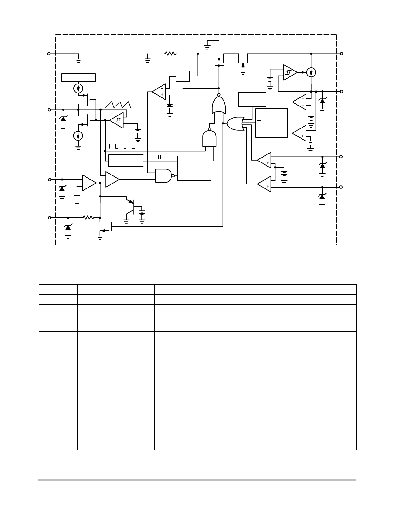
NCP1030, NCP1031
GND
RSENSE
Internal Bias
Current Limit
Comparator
LEB
I1
CT Ramp
+
CT
50 mV
−
10 V
I2 = 3I1
+
3.0 V/3.5 V −
Error Amplifier
VFB
−
+
10 V +
2.5 V
−
I
One Shot
Pulse
O
−
+
PWM Comparator
S Reset Q
Dominant
R Latch
PWM Latch
COMP
2 kW
10 V
4.5 V
VDRAIN
+
7.5 V/10 V
−
Disable
ISTART
VCC
Thermal
Shutdown
16 V
Reset S
Q Dominant
Latch
+
10 V−
R
+
6.5 V
−
UV
+
10 V
2.5 V
−
OV
10 V
Figure 1. NCP1030/31 Functional Block Diagram
FUNCTIONAL PIN DESCRIPTION
Pin Name
Function
1 GND
Ground
2
CT
Oscillator Frequency
Selection
3
VFB
Feedback Input
4 COMP Error Amplifier Compensation
5
OV
Line Overvoltage Shutdown
6
UV
Line Undervoltage Shutdown
7
VCC
Supply Voltage
8 VDRAIN
Power Switch and
Startup Circuits
Description
Ground reference pin for the circuit.
An external capacitor connected to this pin sets the oscillator frequency up to 1 MHz.
The oscillator can be synchronized to a higher frequency by charging or discharging
CT to trip the internal 3.0 V/3.5 V comparator. If a fault condition exists, the power
switch is disabled and the frequency is reduced by a factor of 7.
The regulated voltage is scaled down to 2.5 V by means of a resistor divider.
Regulation is achieved by comparing the scaled voltage to an internal 2.5 V reference.
Requires external compensation network between COMP and VFB pins. This pin is
effectively grounded if faults are present.
Line voltage (Vin) is scaled down using an external resistor divider such that the OV
voltage reaches 2.5 V when line voltage reaches its maximum operating voltage.
Line voltage is scaled down using an external resistor divider such that the UV
voltage reaches 2.5 V when line voltage reaches its minimum operating voltage.
This pin is connected to an external capacitor for energy storage. During Turn−On, the
startup circuit sources current to charge the capacitor connected to this pin. When the
supply voltage reaches VCC(on), the startup circuit turns OFF and the power switch is
enabled if no faults are present. An external winding is used to supply power after
initial startup to reduce power dissipation. VCC should not exceed 16 V.
This pin directly connects the Power Switch and Startup Circuits to one of the
transformer windings. The internal High Voltage Power Switch Circuit is connected
between this pin and ground. VDRAIN should not exceed 200 V.
http://onsemi.com
2
Share Link: