NC33395T Ver la hoja de datos (PDF) - Motorola => Freescale
Número de pieza
componentes Descripción
Fabricante
NC33395T Datasheet PDF : 16 Pages
| |||
Freescale Semiconductor, Inc.
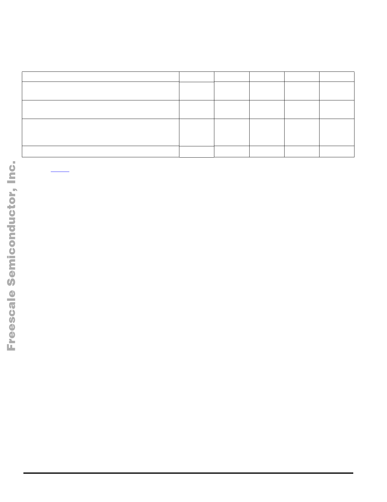
DYNAMIC ELECTRICAL CHARACTERISTICS
Characteristics noted under conditions -40°C ≤ TA ≤ 125°C, 5.5 V ≤ VIGNP ≤ 24 V unless otherwise noted. Typical values reflect
approximate parameter mean at TA = 25°C under normal conditions unless otherwise noted.
Characteristic
Symbol
Min
Typ
Max
Unit
High-Side (GDHn) and Low-Side Drivers (GDHn) Rise Time
(25% to 75%), CISS Value = 2000 pF (Note 7)
t RH
µs
–
0.35
1.5
High-Side (GDHn) and Low-Side Drivers (GDHn) Fall Time
(75% to 25%), CISS Value = 2000 pF (Note 7)
t FH
µs
–
0.25
1.5
Shoot-Through Suppression Time Delay (33395) (Note 7), (Note 8)
t D1, t D2
µs
33395
1.0
3.0
5.5
33395T
0.2
0.65
1.0
Current Limit Time Delay (Note 9)
t ILIMDELAY
1.5
2.8
5.0
µs
Notes
7. See Figure 2, page 9.
8. Shoot-Through Suppression Time Delay is provided to prevent directly connected high- and low-side MOSFETs from being on
simultaneously.
9. Current Limit Time Delay: The internal comparator places the device in the current limit mode when the comparator output goes LOW and
sets an internal logic bit. This takes a finite amount of time and is stated as the Current Limit Time Delay.
33395
8
For More Information OMnOTTOhRiOsLPArAoNdAuLOcGt,INTEGRATED CIRCUIT DEVICE DATA
Go to: www.freescale.com
Share Link: 