CXK5B18120TM Ver la hoja de datos (PDF) - Sony Semiconductor
N√∫mero de pieza
componentes Descripción
Fabricante
CXK5B18120TM Datasheet PDF : 10 Pages
| |||
CXK5B18120TM
Electrical Characteristics
DC Characteristics
Item
Symbol
(Vcc = 3.3V±0.3V, GND = 0V, Ta = 0 to +70°C)
Conditions
Min. Typ.‚àó Max. Unit
Input leakage current ILI
VIN = GND to Vcc
–10
—
+10 µA
Output leakage current ILO
CE = VIH or OE = VIH or WE = VIL or
UB = VIH or LB = VIH
VI/O = GND to Vcc
–10
—
+10 µA
Average operating
current
Min. Cycle
ICC
Duty =100%
IOUT = 0mA, CE = VIL, VIN = VIH or VIL
—
—
310 mA
Standby current
ISB1
CE ≥ Vcc – 0.2V
VIN ≥ Vcc – 0.2V or VIN ≤ 0.2V
Min. Cycle
ISB2
Duty =100%
CE = VIH, VIN = VIH or VIL
—
—
10 mA
—
—
100 mA
Output high voltage
VOH IOH = –2.0mA
2.4
—
—V
Output low voltage
VOL
IOL = 2.0mA
—
—
0.4 V
* Vcc = 3.3V, Ta = 25°C
I/O Capacitance
(Ta = 25°C, f = 1MHz)
Item
Symbol Conditions Min.
Input capacitance CIN
VIN = 0V
—
I/O capacitance
CI/O
VI/O = 0V
—
Typ.
—
—
Max. Unit
5 pF
7 pF
Note) This parameter is sampled and is not 100% tested.
AC Characteristics
• AC test condition (Vcc = 3.3V±0.3V, Ta = 0 to +70°C)
Item
Input pulse high level
Input pulse low level
Input rise time
Input fall time
Input and output reference level
Output load conditions
Condition
VIH = 3.0V
VIL = 0.0V
tr = 2ns
tf = 2ns
1.4V
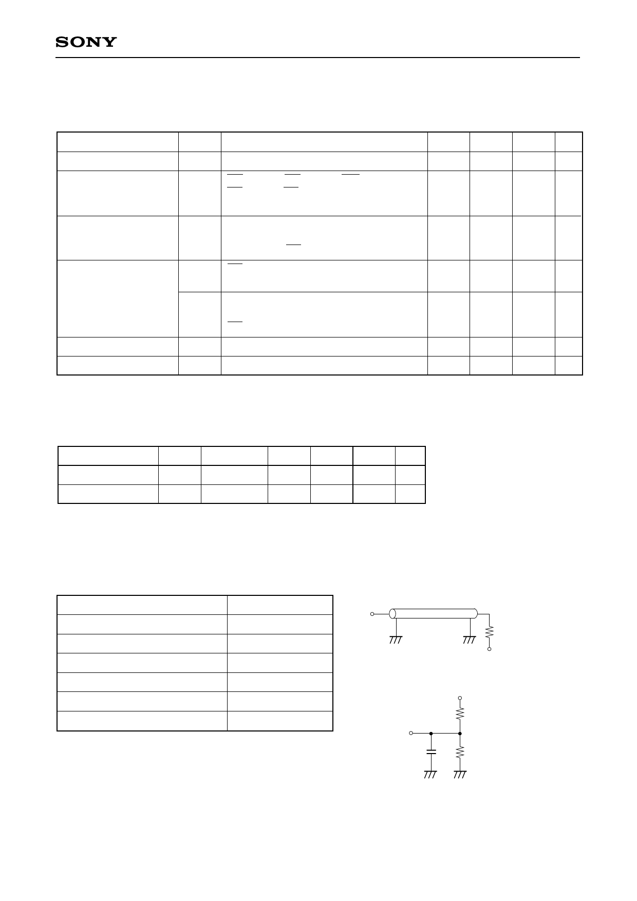
Fig. 1
Output load (1)
I/O
Zo=50Ω
RL=50Ω
VL=1.4V
Output load (2)*1
3.3V
1179Ω
I/O
5pF*2
868Ω
*1. For tLZ, tOLZ, tLBLZ, tUBLZ, tHZ, tOHZ, tLBHZ, tUBHZ, tOW, tWHZ
*2. Including scope and jig capacitances.
Fig. 1
–3–
Share Link: 