MXB7846(2004) Ver la hoja de datos (PDF) - Maxim Integrated
Número de pieza
componentes Descripción
Fabricante
MXB7846
(Rev.:2004)
(Rev.:2004)
MXB7846 Datasheet PDF : 23 Pages
| |||

2.375V to 5.25V, 4-Wire Touch-Screen Controller
with Internal Reference and Temperature Sensor
ABSOLUTE MAXIMUM RATINGS
VDD, VBAT, DIN, CS, DCLK to GND ........................-0.3V to +6V
Digital Outputs to GND...............................-0.3V to (VDD + 0.3V)
VREF, X+, X-, Y+, Y-, AUX to GND..............-0.3V to (VDD + 0.3V)
Maximum Current into Any Pin .........................................±50mA
Maximum ESD per IEC-61000-4-2 (per MIL STD-883 HBM)
X+, X-, Y+, Y-, VBAT, AUX ......................................15kV (4kV)
All Other Pins ..........................................................2kV (500V)
Continuous Power Dissipation (TA = +70°C)
16-Pin QSOP (derate 8.30mW/°C above +70°C).........667mW
16-Pin TSSOP (derate 5.70mW/°C above +70°C) .......456mW
Operating Temperature Range ...........................-40°C to +85°C
Junction Temperature ......................................................+150°C
Storage Temperature Range .............................-65°C to +150°C
Lead Temperature (soldering, 10s) .................................+300°C
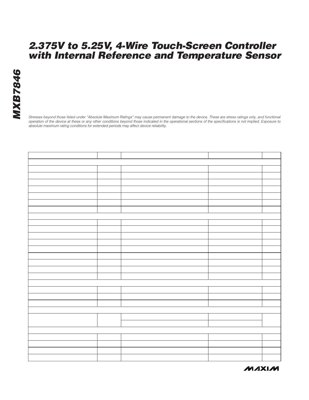
Stresses beyond those listed under “Absolute Maximum Ratings” may cause permanent damage to the device. These are stress ratings only, and functional
operation of the device at these or any other conditions beyond those indicated in the operational sections of the specifications is not implied. Exposure to
absolute maximum rating conditions for extended periods may affect device reliability.
ELECTRICAL CHARACTERISTICS
(VDD = 2.7V to 3.6V, VREF = 2.5V, fDCLK = 2MHz (50% duty cycle), fSAMPLE = 125kHz, 12-bit mode, 0.1µF capacitor at REF, TA =
TMIN to TMAX, unless otherwise noted. Typical values are at TA = +25°C.)
PARAMETER
SYMBOL
CONDITIONS
MIN TYP MAX UNITS
DC ACCURACY (Note 1)
Resolution
12
Bits
No Missing Codes
11
12
Bits
Relative Accuracy
INL (Note 2)
±1
±2
LSB
Differential Nonlinearity
DNL
±1
LSB
Offset Error
±6
LSB
Gain Error
(Note 3)
±4
LSB
Noise
CONVERSION RATE
Including internal reference
70
µVRMS
Conversion Time
Track/Hold Acquisition Time
Throughput Rate
Multiplexer Settling Time
tCONV
tACQ
fSAMPLE
12 clock cycles (Note 4)
3 clock cycles
16 clock conversion
6
µs
1.5
µs
125
kHz
500
ns
Aperture Delay
30
ns
Aperture Jitter
100
ps
Channel-to-Channel Isolation
Serial Clock Frequency
fDCLK
VIN = 2.5VP-P at 50kHz
100
dB
0.1
2.0
MHz
Duty Cycle
40
60
%
ANALOG INPUT (X+, X-, Y+, Y-, AUX)
Input Voltage Range
Input Capacitance
0
VREF
V
25
pF
Input Leakage Current
SWITCH DRIVERS
On/off leakage, VIN = 0 to VDD
±0.1
±1
µA
On-Resistance (Note 5)
Y+, X+
Y-, X-
7
Ω
9
INTERNAL REFERENCE
Reference Output Voltage
REF Output Tempco
VREF VDD = 2.7V to 5.25V, TA = +25°C
TCVREF
2.45 2.50 2.55
V
50
ppm°/C
REF Short-Circuit Current
18
mA
REF Output Impedance
250
Ω
2 _______________________________________________________________________________________