MX25L4005AMC Ver la hoja de datos (PDF) - Macronix International
Número de pieza
componentes Descripción
Fabricante
MX25L4005AMC Datasheet PDF : 44 Pages
| |||
MX25L4005A
• HOLD# pin
- pause the chip without diselecting the chip
• PACKAGE
- 8-pin SOP (150mil)
- 8-pin SOP (200mil)
- 8-pin PDIP (300mil)
- 8-land SON (6x5mm, 1.0mm package height), which is not recommended for new design
- 8-land WSON (6x5mm, 0.8mm package height)
- 8-land USON (4x4mm) in development
- All Pb-free devices are RoHS Compliant
GENERAL DESCRIPTION
The MX25L4005A is a CMOS 4,194,304 bit serial Flash memory, which is configured as 524,288 x 8 internally. The
MX25L4005A feature a serial peripheral interface and software protocol allowing operation on a simple 3-wire bus. The three
bus signals are a clock input (SCLK), a serial data input (SI), and a serial data output (SO). SPI access to the device is
enabled by CS# input.
The MX25L4005A provide sequential read operation on whole chip.
After program/erase command is issued, auto program/ erase algorithms which program/ erase and verify the specified
page or byte /sector/block locations will be executed. Program command is executed on page (256 bytes) basis, and erase
command is executes on chip or sector(4K-bytes) or block(64K-bytes).
To provide user with ease of interface, a status register is included to indicate the status of the chip. The status read
command can be issued to detect completion status of a program or erase operation via WIP bit.
When the device is not in operation and CS# is high, it is put in standby mode and draws less than 10uA DC current.
The MX25L4005A utilize MXIC's proprietary memory cell, which reliably stores memory contents even after 100,000
program and erase cycles.
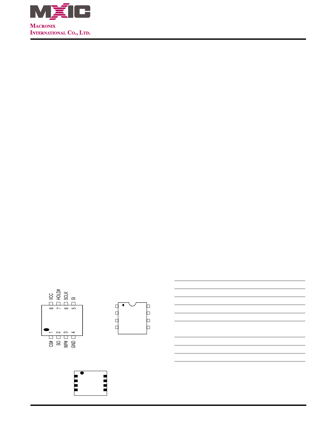
PIN CONFIGURATIONS
PIN DESCRIPTION
8-PIN SOP (150/200mil) 8-PIN PDIP (300mil)
CS# 1
SO 2
WP# 3
GND 4
8 VCC
7 HOLD#
6 SCLK
5 SI
*8-LAND SON (6x5mm), WSON (6x5mm), USON (4x4mm)
SYMBOL
CS#
SI
SO
SCLK
HOLD#
WP#
VCC
GND
DESCRIPTION
Chip Select
Serial Data Input
Serial Data Output
Clock Input
Hold, to pause the device without
deselecting the device
Write Protection
+ 3.3V Power Supply
Ground
CS# 1
SO 2
WP# 3
GND 4
8 VCC
7 HOLD#
6 SCLK
5 SI
Note: 8-land SON is not recommended for new design
P/N: PM1231
2
REV. 1.8, JUL. 17, 2008
Share Link: 