MV8870 Ver la hoja de datos (PDF) - Unspecified
Número de pieza
componentes Descripción
Fabricante
MV8870 Datasheet PDF : 13 Pages
| |||
MV8870/MV8870-1
FUNCTIONAL DESCRIPTION
The MV8870 / MV8870-1 monolithic DTMF receiver offers
small size, low power consumption and high performance. Its
architecture consists of a bandsplit filter section, which
separates the high and low tone groups, followed by a digital
counting section which verifies the frequency and duration of
the received tones before passing the corresponding code to
the output bus.
FILTER SECTION
Separation of the low-group and high-group tones is
achieved by applying the DTMF signal to the inputs of two
sixth-order switched capacitor band-pass filters, the
bandwidths of which correspond to the low and high group
frequencies. The filter section also incorporates notches at 350
and 440 Hz for exceptional dial tone rejection (see Fig.3). Each
filter is followed by a single order switched capacitor filter
section which smooths the signals prior to limiting. Limiting is
performed by high-gain comparators which are provided with
hysteresis to prevent detection of unwanted low-level signals.
The outputs of the comparators provide full rail logic swings at
the trequencies of the incoming DTMF signals.
For testing and monitoring, the high and low group filter
and zero crossing detector outputs are made available via
FHT, FH, FLT and FL (HP package only).
DECODER SECTION
Following the filter section is a decoder employing digital
counting techniques to determine the frequencies ot the
incoming tones and to verify that they correspond to standard
DTMF frequencies. A complex averaging algorithm protects
against tone simulation by extraneous signals such as voice
while providing tolerance to small frequency deviations and
variations. This averaging algorithm has been developed to
ensure an optimum combination of immunity to talk-off and
tolerance to the presence of interfering frequencies (third
tones) and noise. When the detector recognises the
simultaneous presence of two valid tones (this is referred to as
the ‘Signal Condition’ in some industry specifications) the Early
Steering output (ESt) will go to an active state. Any
subsequent loss of signal condition will cause the ESt pin to go
to its inactive state (see Fig.5).
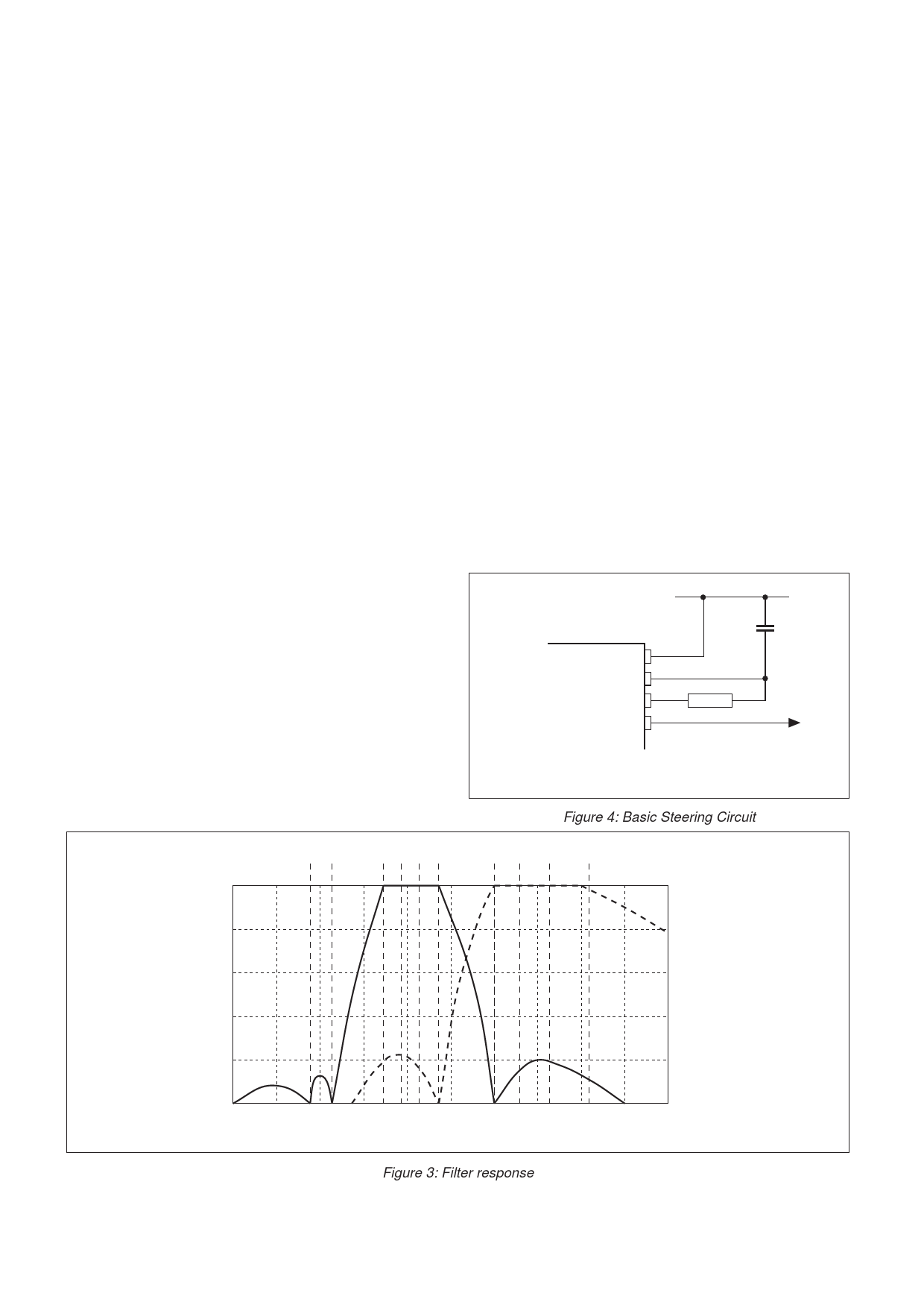
STEERING CIRCUIT
Before registration of a decoded tone-pair, the receiver
checks for a valid signal duration (referred to as (character
recognition condition). This check is performed by an external
RC time constant driven by ESt. A logic high on ESt causes the
voltage at the SVGT pin (VSt/GT) to rise as the capacitor
discharges (see Figs.4 and 5).
Provided signal condition is maintained (ESt remains high)
for the validation period (tGTP), VSUGT reaches the threshold
(VTSt) of the steering logic which allows it to register the tone
pair and strobe the corresponding 4-bit code into the output
latch (see Fig.6). At this point the SVGT pin is activated as an
output and drives VSt/GT to VDD (see Fig.5).
St/GT continues to drive high as long as ESt remains high.
After a short delay (tDP) to allow the output latch to settle, the
delayed steering output pin (StD) goes high to indicate that the
code for a new received tone-pair is available. The contents of
the output latch are output onto the output bus (Q1 to Q4 pins)
when the three-state output enable (TOE) pin is high.
The steering circuit works in reverse to validate the
interdigit pause between signals. Thus as well as rejecting
signals too short to be considered valid, the receiver will
tolerate signal interruptions (drop-out) too short to be
considered a valid pause. This facility, together with the
capability of selecting the steering time constants externally,
allows the designer to tailor performance to meet a wide
variety of system requirements.
VDD
18
VDD
MV8870/ St/GT
MV8870-1 ESt
17
16
StD 15
C
R
tGTA = RC In {VDD ÷ VTSI}
tGTP = RC In {VDD ÷ (VDD - VTSU)}
Figure 4: Basic Steering Circuit
0
10
20
ATTENUATION
(dB)
30
40
50
XY
ABC D
EF G
H
200 400 600
800 1000 1200
FREQUENCY (Hz)
1400 1600
1800
2000
Precise
Dial Tones
X = 350 Hz
Y = 440 Hz
DTMF Tones
A = 697 Hz
B = 770 Hz
C = 852 Hz
D = 941 Hz
E = 1209 Hz
F = 1336 Hz
G = 1477 Hz
H = 1633 Hz
2
Figure 3: Filter response
Share Link: 