74LVC841A Ver la hoja de datos (PDF) - Philips Electronics
Número de pieza
componentes Descripción
Fabricante
74LVC841A Datasheet PDF : 10 Pages
| |||
Philips Semiconductors
10-bit transparent latch with 5-volt tolerant
inputs/outputs (3-State)
Product specification
74LVC841A
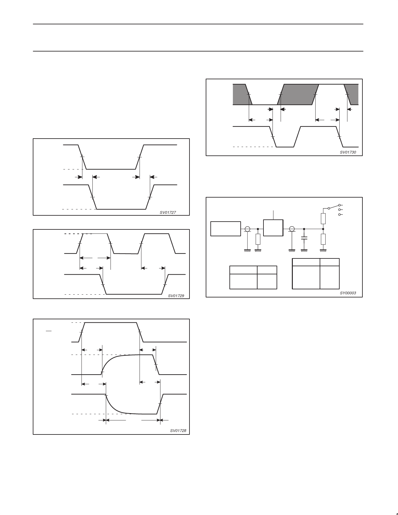
AC WAVEFORMS
VM = 1.5 V at VCC ≥ 2.7 V
VM = 0.5 V × VCC at VCC < 2.7 V
VM = 1.5 V at VCC = 3.0 V
VOL and VOH are the typical output voltage drop that occur with the
output load.
VX = VOL + 0.3 V at VCC ≥ 2.7 V
VX = VOL + 0.1 × VCC at VCC < 2.7 V
VY = VOH – 0.3 V at VCC ≥ 2.7 V
VY = VOH – 0.1 × VCC at VCC < 2.7 V
VI
Dn Input
VM
GND
VOH
tPHL
tPLH
Qn Output
VM
VOL
SV01727
Figure 1. Input (Dn) to output (Qn) propagation delays.
VI
LE INPUT
VM
GND
tW
VOH
t PHL
t PLH
Qn OUTPUT
VM
VOL
SV01729
Figure 2. Latch enable input (LE) pulse width, the latch enable
input to output (Qn) propagation delays.
VI
OE INPUT
GND
VCC
Qn OUTPUT
LOW-to-OFF
OFF-to-LOW
VOL
VM
tPLZ
VX
tPHZ
tPZL
VM
tPZH
VOH
Qn OUTPUT
HIGH-to-OFF
OFF-to-HIGH
GND
VY
outputs
enabled
outputs
disabled
VM
outputs
enabled
SV01728
Figure 3. 3-State enable and disable times.
VI
Dn INPUT
VM
GND
th
th
t su
tsu
VI
LE INPUT
VM
GND
SV01730
Figure 4. Data set-up and hold times for the
Dn input to LE input.
Note to Figure 4: The shaded areas indicate when the input is
permitted to change for predictable output performance
TEST CIRCUIT
VI
PULSE
GENERATOR
VCC
D.U.T.
RT
VO
CL 50pF
S1
500Ω
2 x VCC
Open
GND
500Ω
VCC
t 2.7V
2.7V – 3.6V
VI
VCC
2.7V
Test
tPLH/tPHL
tPLZ/tPZL
tPHZ/tPZH
S1
Open
2 x VCC
GND
SY00003
Figure 5. Load circuitry for switching times.
1998 Jun 17
6
Share Link: 