NM25C640 Ver la hoja de datos (PDF) - Fairchild Semiconductor
Número de pieza
componentes Descripción
Fabricante
NM25C640
Fairchild Semiconductor

NM25C640 Datasheet PDF : 10 Pages
| |||
Functional Description (Continued)
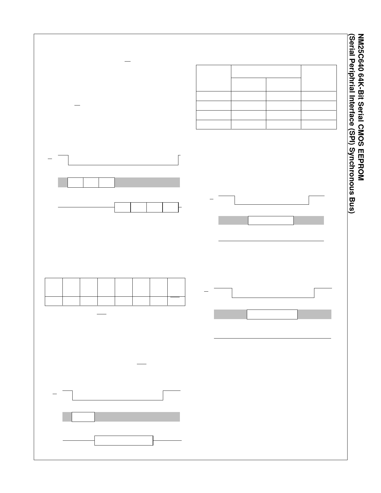
READ SEQUENCE: Reading the memory via the serial SPI link TABLE 3. Block Write Protection Levels
requires the following sequence. The CS line is pulled low to select
the device. The READ op-code is transmitted on the SI line
Level Status Register Bits Array
followed by the high order address byte (A12–A8), and the low
Address
order address byte (A7–A0). The leading three bits in the high
BP1
BP0 Protected
order address byte will be ignored. After this is done, data on the
SI line becomes don’t care. The data (D7–D0) at the address
0
0
0
None
specified is then shifted out on the SO line. If only one byte is to
1
0
1
1800-1FFF
be read, the CS line can be pulled back to the high level. It is
possible to continue the READ sequence as the byte adress is
2
1
0
1000-1FFF
automatically incremented and data will continue to be shifted out.
3
1
1
0000–1FFF
When the highest address is reached (1FFF), the address counter
rolls over to lowest address (000) allowing the entire memory to be
read in one continuous READ cycle. See Figure 6.
WRITE ENABLE (WREN): When VCC is applied to the chip, it
“powers up” in the write disable state. Therefore, all programming
FIGURE 6. Read Sequence
CS
Read Byte H Byte L
SI
Op-Code Addr. n Addr. n
modes must be preceded by a WRITE ENABLE (WREN) instruc-
tion. Additionally, the WP must be held high during a write engble
instruction. At the completion of a WRITE or WRSR cycle the
device is automatically returned to the write disable state. Note
that a WRITE DISABLE (WRD) instruction will also return the
device to the write disable state. See Figure 8.
FIGURE 8. Write Enable
CS
SO
Data Data Data Data
n
n+1 n+2 n+3
DS500041-8
SI
READ STATUS REGISTER (RDSR) : The Read Status Register
(RDSR) instruction provides access to the status register is used
to interrogate the READY/BUSY and WRITE ENABLE status of
SO
WREN Op-Code
DS500041-10
the chip. Two non-volatile status register bits are used to select
one of four levels of BLOCK WRITE PROTECTION. The status WRITE DISABLE (WRDI): To protect against accidental data
register format is shown in Table 2.
disturbance the WRITE DISABLE (WRDI) instruction disables all
TABLE 2. Status Register Format
programming modes. See Figure 9.
Bit Bit Bit Bit Bit Bit Bit Bit
7 65 43 210
X
X
X
X BP1 BP0 WEN RDY
X = Don't Care.
Status register Bit 0 = 0 (RDY) indicates that the device is READY;
Bit 0 = 1 indicates that a program cycle is in progress. Bit 1 = 0
(WEN) indicates that the device is not WRITE ENABLED; Bit 1 =
1 indicates that the device is WRITE ENABLED. Non-volatile
status register Bits 2 and 3 (BP0 and BP1) indicate the level of
FIGURE 9. Write Disable
CS
SI
WRDI Op-Code
SO
DS500041-11
BLOCK WRITE PROTECTION selected. The block write protec-
tion levels and corresponding status register control bits are
shown in Table 3. Note that if a RDSR instruction is executed
during a programming cycle only the RDY bit is valid. All
other bits are 1s. See Figure 7.
FIGURE 7. Read Status
CS
RDSR
SI
Op-Code
SO
SR Data
MSB…LSB
DS500041-9
NM25C640 Rev. D.2
7
www.fairchildsemi.com
Share Link: