28LV64A Ver la hoja de datos (PDF) - Microchip Technology
Número de pieza
componentes Descripción
Fabricante
28LV64A Datasheet PDF : 8 Pages
| |||
28LV64A
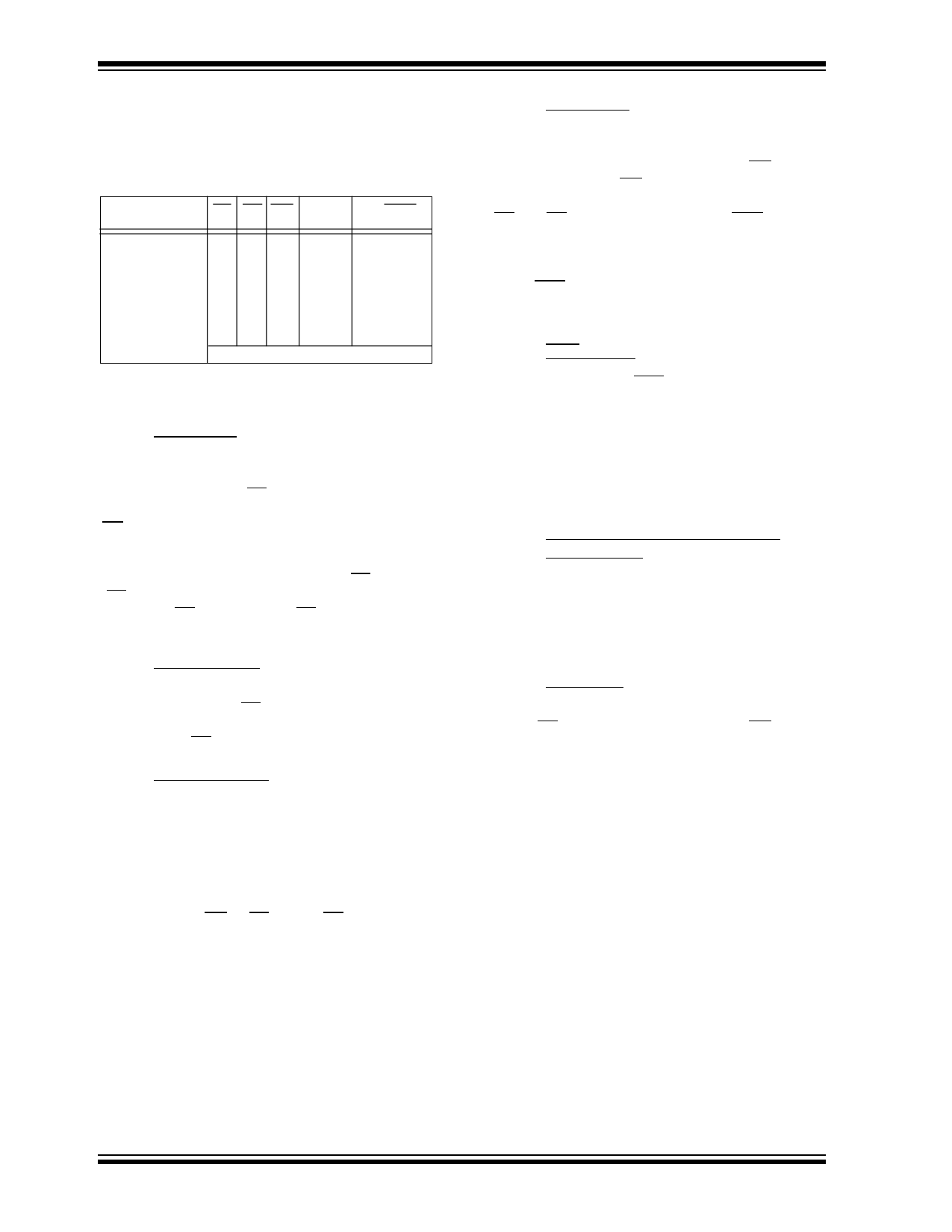
2.0 DEVICE OPERATION
The Microchip Technology Inc. 28LV64A has four
basic modes of operation—read, standby, write inhibit,
and byte write—as outlined in the following table.
Operation Mode CE OE WE I/O Rdy/Busy(1)
Read
L L H DOUT H
Standby
H X X High Z H
Write Inhibit
H X X High Z H
Write Inhibit
X L X High Z H
Write Inhibit
X X H High Z H
Byte Write
L H L DIN L
Byte Clear
Automatic Before Each "Write"
Note: (1) Open drain output.
2.1 Read Mode
The 28LV64A has two control functions, both of which
must be logically satisfied in order to obtain data at the
outputs. Chip enable (CE) is the power control and
should be used for device selection. Output Enable
(OE) is the output control and is used to gate data to
the output pins independent of device selection.
Assuming that addresses are stable, address access
time (tACC) is equal to the delay from CE to output
(tCE). Data is available at the output tOE after the fall-
ing edge of OE, assuming that CE has been low and
addresses have been stable for at least tACC-tOE.
2.2 Standby Mode
The 28LV64A is placed in the standby mode by apply-
ing a high signal to the CE input. When in the standby
mode, the outputs are in a high impedance state, inde-
pendent of the OE input.
2.3 Data Protection
In order to ensure data integrity, especially during criti-
cal power-up and power-down transitions, the follow-
ing enhanced data protection circuits are incorporated:
First, an internal VCC detect (2.0 volts typical) will
inhibit the initiation of non-volatile programming opera-
tion when VCC is less than the VCC detect circuit trip.
Second, holding WE or CE high or OE low, inhibits a
write cycle during power-on and power-off (VCC).
2.4 Write Mode
The 28LV64A has a write cycle similar to that of a
static RAM. The write cycle is completely self-timed
and initiated by a low going pulse on the WE pin. On
the falling edge of WE, the address information is
latched. On rising edge, the data and the control pins
(CE and OE) are latched. The Ready/Busy pin goes
to a logic low level indicating that the 28LV64A is in a
write cycle which signals the microprocessor host that
the system bus is free for other activity. When
Ready/Busy goes back to a high, the 28LV64A has
completed writing and is ready to accept another
cycle.
2.5 Data Polling
The 28LV64A features Data polling to signal the com-
pletion of a byte write cycle. During a write cycle, an
attempted read of the last byte written results in the
data complement of I/O7 (I/O0 to I/O6 can not be
determined). After completion of the write cycle, true
data is available. Data polling allows a simple
read/compare operation to determine the status of the
chip eliminating the need for external hardware.
2.6 Electronic Signature for Device
Identification
An extra row of 32 bytes of EEPROM memory is avail-
able to the user for device identification. By raising A9
to 12V ±0.5V and using address locations 1FEO to
1FFF, the additional bytes can be written to or read
from in the same manner as the regular memory array.
2.7 Chip Clear
All data may be cleared to 1's in a chip clear cycle by
raising OE to 12 volts and bringing the WE and CE
low. This procedure clears all data, except for the
extra row.
DS21113B-page 6
Preliminary
© 1996 Microchip Technology Inc.
Share Link: 