FST3383 Ver la hoja de datos (PDF) - Fairchild Semiconductor
Número de pieza
componentes Descripción
Fabricante
FST3383 Datasheet PDF : 5 Pages
| |||
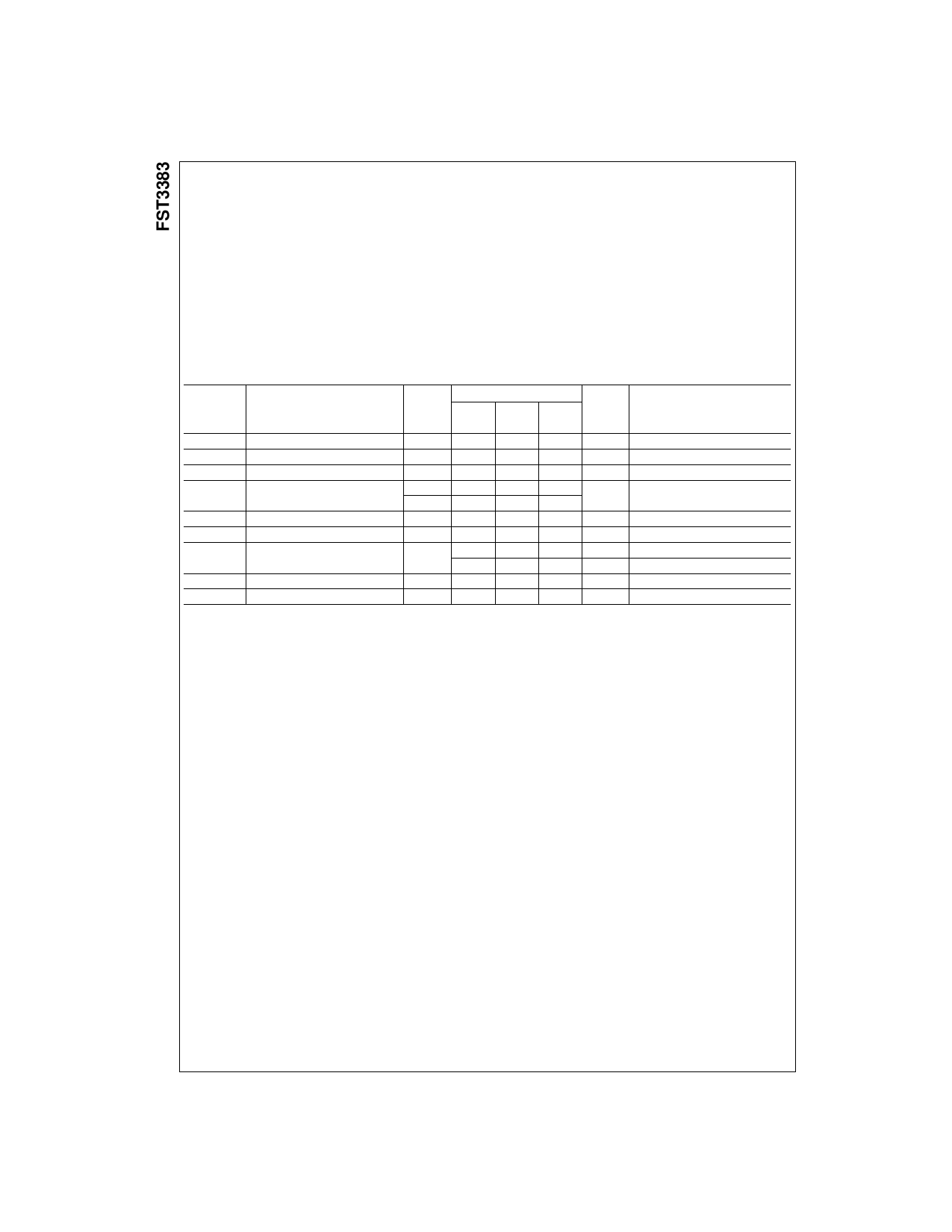
Absolute Maximum Ratings(Note 1)
Supply Voltage (VCC)
DC Switch Voltage (VS)
DC Input Voltage (VI) (Note 2)
DC Input Diode Current (IIN)
with VI < 0
DC Output (IO) Sink Current
Storage Temperature Range (TSTG)
Power Dissipation
−0.5V to +7.0V
−0.5V to +7.0V
−0.5V to +7.0V
−20 mA
120 mA
−65°C to +150°C
0.5W
Recommended Operating
Conditions
Supply Voltage (VCC)
Free Air Operating Temperature (TA)
4.0V to 5.5V
−40°C to +85°C
Note 1: The “Absolute Maximum Ratings” are those values beyond which
the safety of the device cannot be guaranteed. The device should not be
operated at these limits. The parametric values defined in the Electrical
Characteristics tables are not guaranteed at the absolute maximum ratings.
The “Recommended Operating Conditions” table will define the conditions
for actual device operation.
Note 2: The input and output negative voltage ratings may be exceeded if
the input and output diode current ratings are observed.
DC Electrical Characteristics
Symbol
Parameter
TA = −40°C to +85°C
VCC
(V)
Min
Typ
Max
Units
(Note 3)
Conditions
VIK
Maximum Clamp Diode Voltage
4.75
VIH
Minimum High Level Input Voltage 4.75–5.25 2.0
VIL
Maximum Low Level Input Voltage 4.75–5.25
IIN
Maximum Input
0
Leakage Current
5.25
−1.2
V
IIN = −18 mA
V
0.8
V
10
µA 0 ≤ VIN ≤ 5.25V
±1
IOZ
Maximum 3-STATE I/O Leakage
5.25
±10
µA 0 ≤ A, B ≤ VCC
IOS
Short Circuit Current
4.75
100
mA VI(A), VI(B) = 0V, VI(B), VI(A) = 4.75V
RON
Switch On Resistance (Note 4)
4.75
5
7
Ω
VI = 0V, ION = 30 mA
10
15
Ω
VI = 2.4V, ION = 15 mA
ICC
Maximum Quiescent Supply Current 5.25
0.2
10
µA VI = VCC, GND, IO = 0
∆ICC
Increase in ICC per Input (Note 5)
5.25
2.5
mA VIN = 3.15V, IO = 0, Per Control Input
Note 3: All typical values are at VCC = 5.0V, TA = 25°C.
Note 4: Measured by voltage drop between A and B pin at indicated current through the switch. On resistance is determined by the lower of the voltages on
the two (A or B) pins.
Note 5: Per TTL driven input (VIN = 3.15V, control inputs only). A and B pins do not contribute to ICC.
www.fairchildsemi.com
2
Share Link: 