MSM9000-XX Ver la hoja de datos (PDF) - Oki Electric Industry
Número de pieza
componentes Descripción
Fabricante
MSM9000-XX Datasheet PDF : 39 Pages
| |||
¡ Semiconductor
FEDL9000B-01
MSM9000B-xx
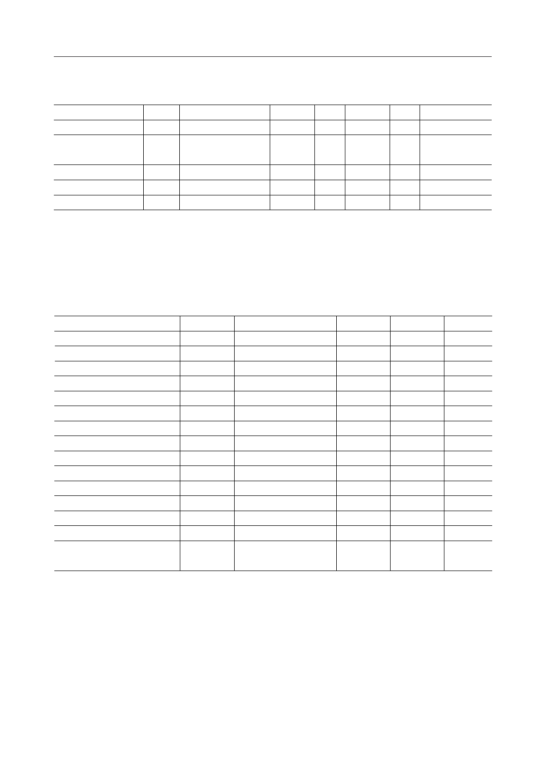
DC Characteristics (2)
Parameter
Bias voltage 1
Symbol
–VSS1
Bias voltages 2 and 3 –VSS2,3
Bias voltage 4
Bias voltage 5
Contrast pitch
–VSS4
–VSS5
–Vcon
Condition
–VSS2, 3 = "A"V
N1 = "L", N2 = "L"
Contrast = "5"
–VSS2, 3 = "A"V
–VSS2, 3 = "A"V
VBI for each stage
Min.
1/2A–0.1
(VDD=0 V, VSS=–3 V, Ta=–30 to +85°C)
Typ. Max. Unit Applicable pin
1/2A 1/2A+0.1 V VSS1
1.9
2.2
2.5
V VSS2, 3
3/2A–0.1 3/2A 3/2A+0.1
2A–0.2 2A 2A+0.2
0.18 0.21 0.26
V VSS4
V VSS5
V
—
Note 1: Connect a 0.1 µF capacitor to the LCD bias generator.
Note 2: The values in this table are assured when the chip is not exposed to light.
AC Characteristics
Parallel interface
Parameter
RD high-level width
RD low-level width
WR high-level width
WR low-level width
WR-RD high-level width
CS or C/D setup time
CS or C/D hold time
Write data setup time
Write data hold time
Read data output delay time
Read data hold time
External clock high-level width
External clock low-level width
RESET pulse width
Rise and fall time of external
clock
Symbol
tWRH
tWRL
tWWH
tWWL
tWWRH
tAS
tAH
tDSW
tDHW
tDDR
tDHR
tWCH
tWCL
tWRE
tr, tf
(VDD=2.5 to 3.3 V, VBI=3 to 5.5 V, Ta=–30 to +85°C)
Condition
Min.
Max.
Unit
—
200
—
ns
—
200
—
ns
—
200
—
ns
—
200
—
ns
—
200
—
ns
—
50
—
ns
—
0
—
ns
—
50
—
ns
—
50
—
ns
CL=50 pF
—
200
ns
—
20
—
ns
—
1
—
ms
—
1
—
ms
—
2.0
—
ms
—
—
100
ns
Note: The values in this table are assured when the chip is not exposed to light.
7/39
Share Link: 