MSM9000-XX Ver la hoja de datos (PDF) - Oki Electric Industry
Número de pieza
componentes Descripción
Fabricante
MSM9000-XX Datasheet PDF : 39 Pages
| |||
¡ Semiconductor
FEDL9000B-01
MSM9000B-xx
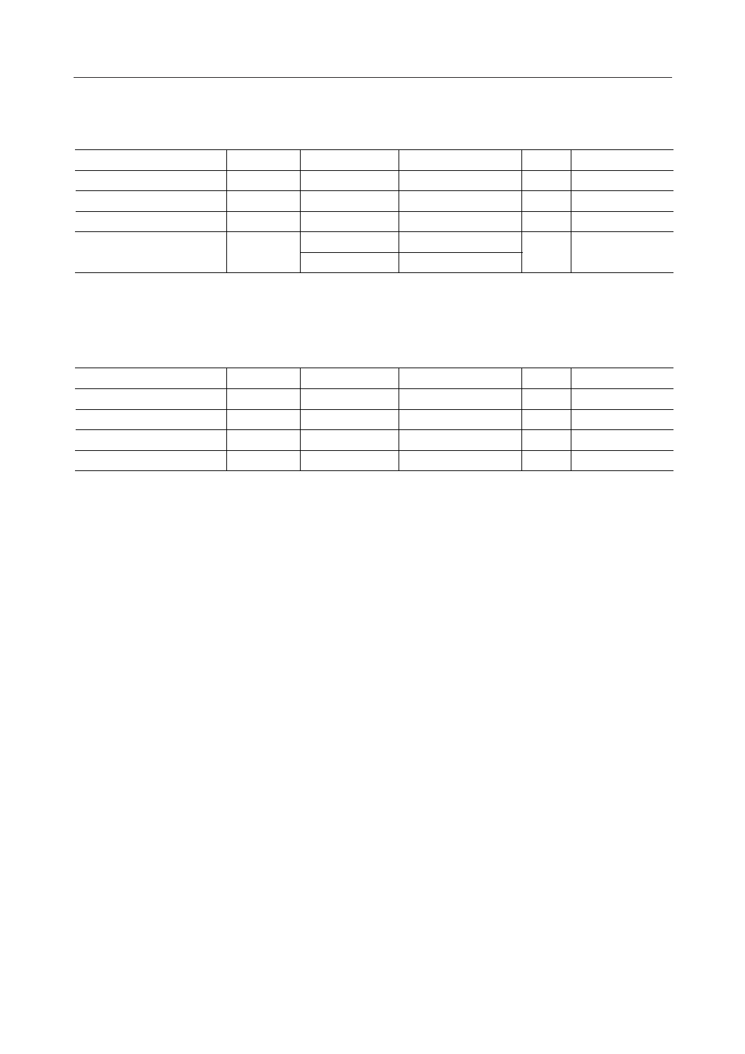
ABSOLUTE MAXIMUM RATINGS
Parameter
Power supply voltage
Bias voltage
Input voltage
Storage temperature
Symbol
VDD
VBI
VI
TSTG
Condition
Ta=25°C, VDD–VSS
Ta=25°C, VDD–VSS5
Ta=25°C
Chip
TCP
Rating
–0.3 to +4.6
–0.3 to +7
–0.3 to VDD + 0.3
–55 to +150
–30 to +85
Ta: Ambient temperature
Unit
V
V
V
Applicable pin
VDD, VSS
VDD, VSS5
All input pins
°C
—
RECOMMENDED OPERATING CONDITIONS
Parameter
Power supply voltage
Bias voltage
IC source oscillation
Operating temperature
Symbol
VDD
VBI
fint
Top
Condition
VDD–VSS
*1, VDD–VSS5
*2
—
Range
2.5 to 3.3
3 to 5.5
26 to 47
–30 to +85
Unit
V
V
kHz
°C
Applicable pin
VDD, VSS
VDD, VSS5
*3
—
*1 VDD is the highest pin and VSS5 the lowest for the bias voltage.
*2 Connect the specified capacitors to the voltage doubler and LCD bias generator.
*3 Make sure that the crystal oscillation frequency or the divided clock frequency falls within
this range.
Note 1: Ensure the chip is not exposed to any light.
Note 2: The bias voltage may exceed 5.5 V at some contrast stages. Adjust the stage with
software so that the bias voltage does not exceed 5.5 V.
5/39
Share Link: 