MSM7650 Ver la hoja de datos (PDF) - Oki Electric Industry
Número de pieza
componentes Descripción
Fabricante
MSM7650 Datasheet PDF : 34 Pages
| |||
¡ Semiconductor
MSM7650
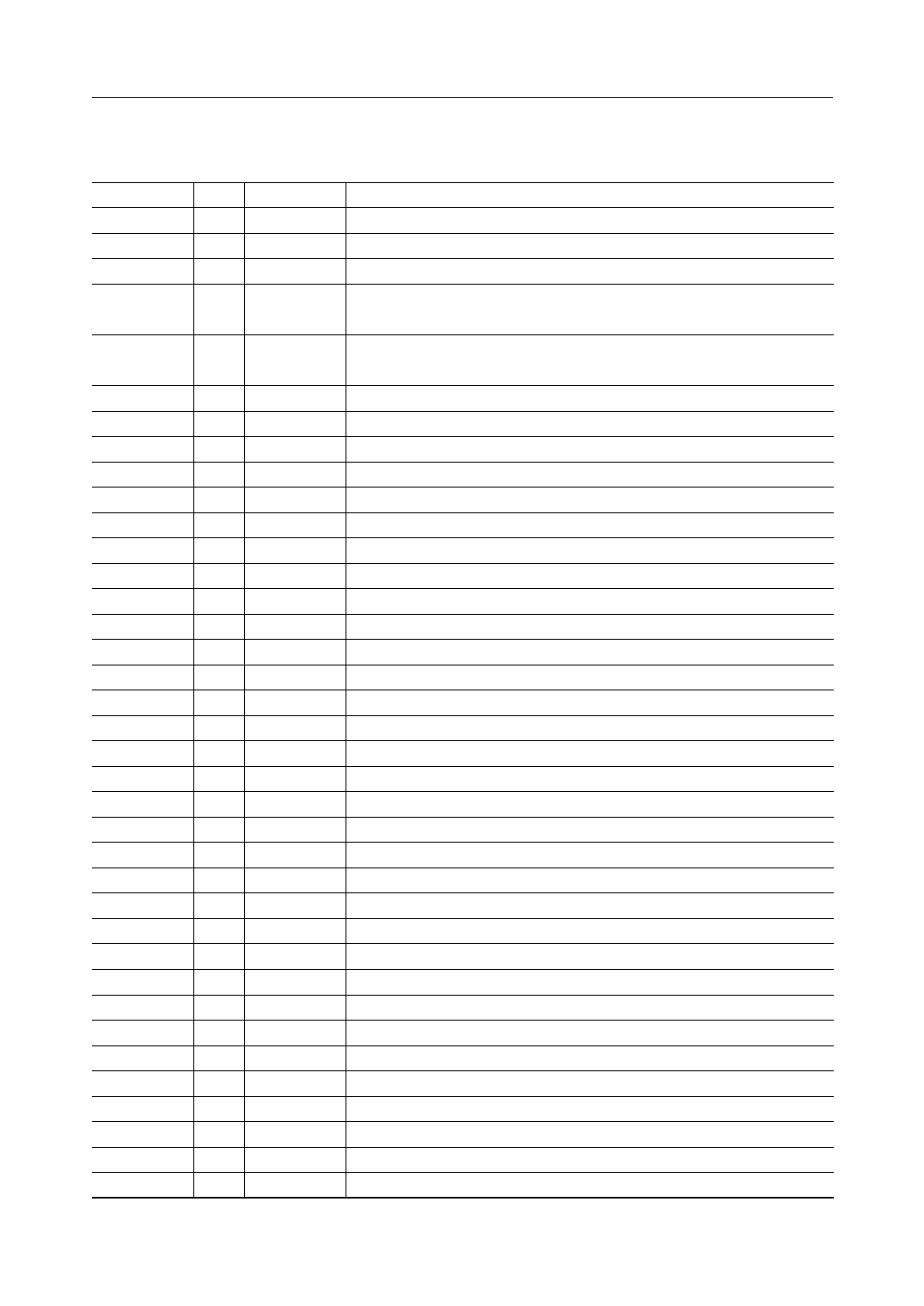
PIN DESCRIPTIONS (1/2)
Pin
1
2
3
4
5
6
7
8
9
10
11
12
13
14 to 22
23
24
25
26
27
28
29
30
31
32
33
34
35
36
37
38
39
40
41
42
43
44
45
I/O Symbol
Description
VDD5
5.0V power supply
VDD3
3.3V power supply
GND Digital GND
I/O VSYNC_L Vertical sync signal
Polarity is negative. Output pin in master mode; input pin in slave mode.
I/O HSYNC_L Horizontal sync signal
Polarity is negative. Output pin in master mode; input pin in slave mode.
I
BLANK_L Composite blank signal. Polarity is negative.
I
CLKX1 Pixel clock input pin
I
CLKX2 Double pixel clock input pin
O
CLKX2O Double pixel clock output pin
I
X
Test pin. Normally, fixed to "0".
O
X_L
Test pin
VDD3
3.3V power supply
GND Digital GND
I CT8 to CT0 Input pin for testing. Normally, fixed to "0" or "1".
VDD5
5.0V power supply
GND Digital GND
VDD3
3.3V power supply
NC
Not connected
I/O
VREF Reference voltage for DAC
I
FS
DAC full scale adjustment pin
I
COMP DAC phase compensation pin
I
AGND Analog GND
O
YA
Analog luminance signal output pin
AGND Analog GND
AVDD Analog power supply
AVDD Analog power supply
O
CVBSO Analog composite video signal output pin
AGND Analog GND
O
CA
Analog chrominance signal output pin
AVDD Analog power supply
GND Digital GND
NC
Not connected
VDD3
3.3V power supply
GND Digital GND
TEST1 Input pin 1 for testing. Normally, fixed to "0".
I
TEST2 Input pin 2 for testing. Normally, fixed to "0".
I
TEST3 Input pin 3 for testing. Normally, fixed to "0".
5/34
Share Link: 