MSM7532 Ver la hoja de datos (PDF) - Oki Electric Industry
Número de pieza
componentes Descripción
Fabricante
MSM7532 Datasheet PDF : 21 Pages
| |||
¡ Semiconductor
MSM7532
CE1, CE2
Pins used to connect a capacitor for removing DC offset in the expander.
Insert a 0.22 mF capacitor between CE1 and SGO, an 1 mF capacitor between CE2 and SGO.
EMP
Emphasis path selection pin.
EMP
0
1
Transmit side
Pre-emphasis circuit is bypassed to the path
Pre-emphasis circuit is connected to the path
Receive side
De-emphasis circuit is bypassed to the path
De-emphasis circuit is connected to the path
Note
SW2
RAIO, RAI
Pins used to constitute RC-active filter on the receive signal input side.
Refer to the TVIO and TVI description.
If the Scrambler circuit is used, using the first order RC-active filter is recommended. In this case,
configure the filter so that either R34 or R35, or both of them, is 60 kW or less.
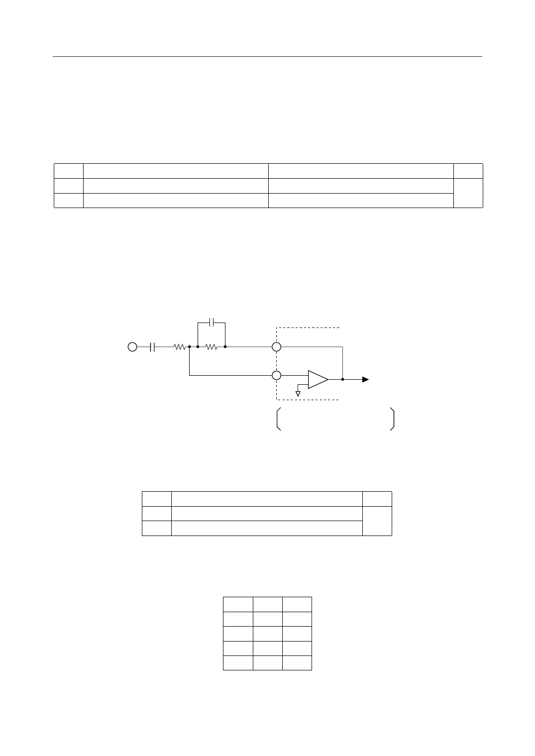
<First order RC-active filter configuration>
C19 R34
C27
R35
RAIO
RAI
–
+
VRAI
In the case of fc = 10 kHz, gain : 0dB
R34 = R35 = 51 kW
C19 = 0.22 mF, C27 = 300 pF
RVO
Receive voice signal output pin.
The RVO state is controlled depending on the digital data set to RVE.
RVE
RVO
Note
0 No signal output (voltage = VSG)
SW7
1 Output of signals input to RAI and RAIO
VOL1, VOL2
Pins used to set up a gain for the electronic volume.
The volume at the stage next to expander is controlled by the pins.
VOL2 VOL1 Gain
0
1 +6 dB
0
0 0 dB
1
1 –6 dB
1
0 –12 dB
CSH
Pin used to connect a capacitor for removing DC offset in shaper of modem receiver.
Insert a 1 mF capacitor between this pin and GND.
9/21
Share Link: 