MSM65514 Ver la hoja de datos (PDF) - Oki Electric Industry
Número de pieza
componentes Descripción
Fabricante
MSM65514 Datasheet PDF : 23 Pages
| |||
¡ Semiconductor
MSM65514/65P514
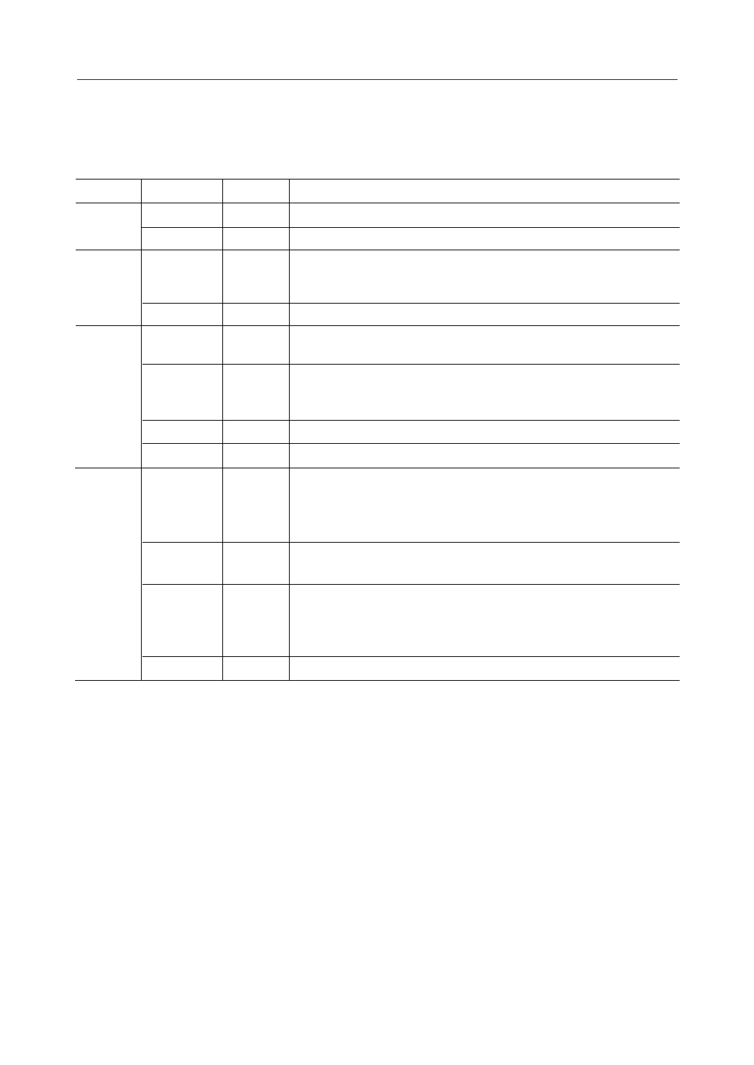
PIN DESCRIPTION
Basic Functions
Function
Power
Supply
Oscillation
Symbol
VDD
GND
OSC0
OSC1
RESET
Type
—
—
I
O
I
EA
I
Control
RD
O
ALE
O
PORT 0
I/O
PORT 1
I/O
Port
PORT 2
I/O
PORT 3
PORT 4
PORT 5
PORT 6
I
Description
+5V power supply
0V ground
System clock input pin. Quartz oscillator or ceramic oscillator is
connected between OSC0 and OSC1. For external clock, input at OSC0,
leaving OSC1 open.
System clock output pin
System reset input (program starts from address 0040H);
internal pull-up resistance
Program memory select input pin.
"L" level input for external program memory; "H" level input for internal
program memory.
Read strobe signal during external memory access
Address latch signal during external memory access
8-bit Input-output port
During external memory access, becomes address/data bus for address
output, instruction fetch or data read/write along with ALE, RD and WR
pins.
8-bit Input-output port
Address bus during external memory access
8-bit Input-output port ¥ 4. Secondary functions shown in following table
are added for ports 2 and 3.
8-bit Input port
6/23
Share Link: 