MSM6595 Ver la hoja de datos (PDF) - Oki Electric Industry
Número de pieza
componentes Descripción
Fabricante
MSM6595 Datasheet PDF : 13 Pages
| |||
¡ Semiconductor
MSM6595A-xxx
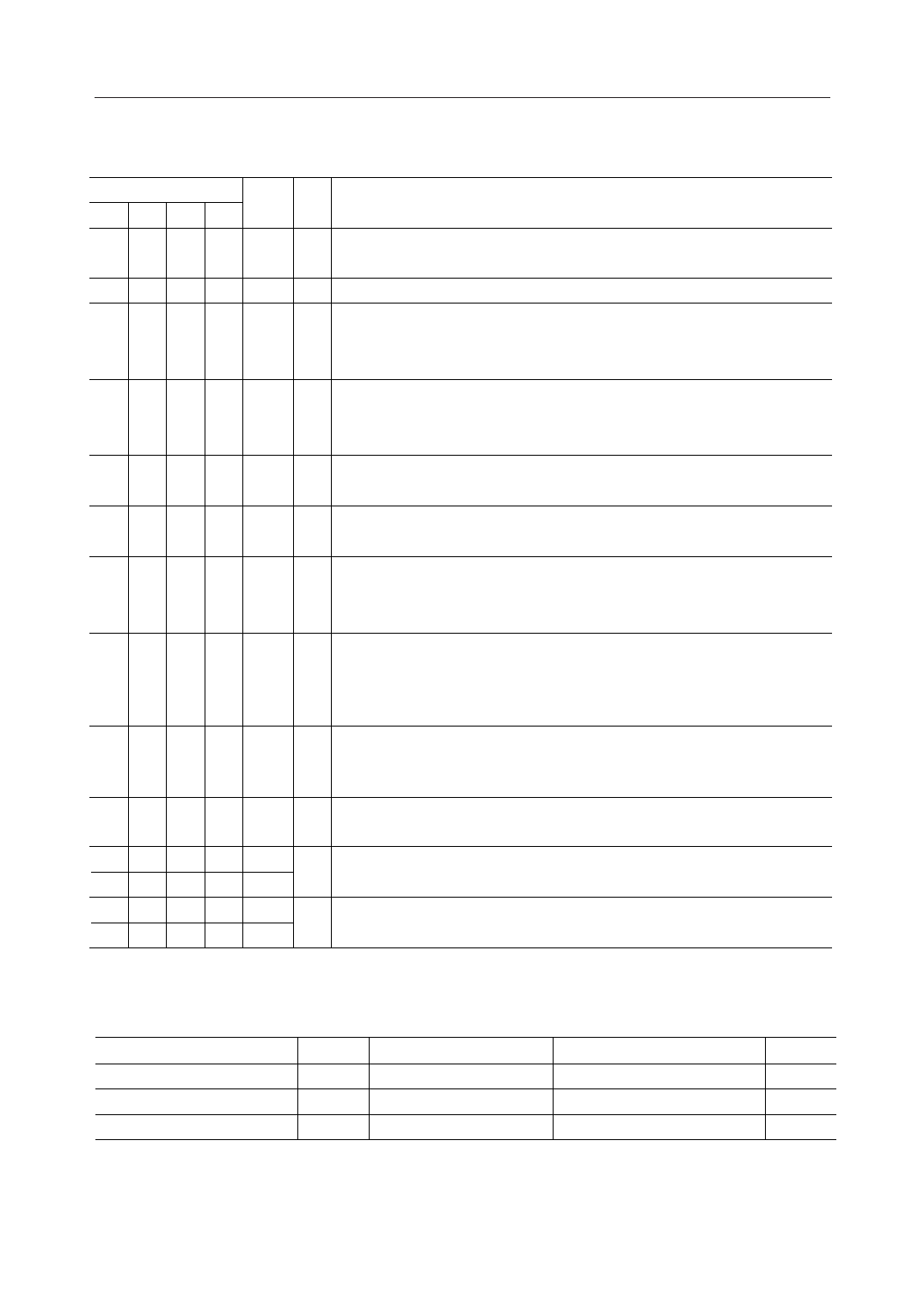
PIN DESCRIPTIONS
Pin
Symbol Type
QFJ SOP DIP SSOP
Description
Power supply pin. Insert a bypass capacitor of 0.1 mF or more between this
9 12 9 15 VDD — pin and the GND pin.
18 24 18 30 GND — Ground pin
(SERIAL ADDRESS) This pin inputs the starting X address of a read operation.
6 9 6 12 SADX I Addressing in units of 1024 words is possible. The 1024-word address data
can be input as 10-bit (AX0 - AX9) serial data via the SADX pin.
(SERIAL ADDRESS) This pin inputs the starting Y address of a read operation.
1 1 1 1 SADY I Addressing in units of 1024 words is possible. The 1024-word address data
can be input as 10-bit (AY0 - AY9) serial data via the SADY pin.
7
10
7
13 SASX
(SERIAL ADDRESS STROBE) This is the clock input pin which is used to store
I the serial address data of the X address into the device's internal register.
2
2
2
2
SASY
I
(SERIAL ADDRESS STROBE) This is the clock input pin to store the serial
address data of the Y address into the device's internal register.
8 11 8
14 TAS
(ADDRESS TRANSFER STROBE) This is the input pin for loading the serial
I address data into the internal address counter.
The X and Y addresses are stored at the falling edge of TAS.
(READ CLOCK) This is the clock input pin for reading information out of the data
13
15
13
18 RDCK
I
register. Internal operation starts at the falling edge of RDCK. The information
in the data register is output on the DOUT pin. The internal address counter is
automatically incremented at the falling edge of RDCK.
(DATA OUT) The data output pin is always kept in a high-impedance state when
17 22 17 28 DOUT O RDCK or CS is kept at "H". This pin reflects the "H" or "L" level data being read,
and the current data is held until RDCK is asserted High.
444
5
CS
(CHIP SELECT) Setting this pin to "H" disables all input and output pins. This pin
I enables parallel use of multiple serial voice ROMs by connecting the data output pins.
10 13 10 16 TEST
3 3 3 3 TEST
I
Pins for testing. Apply a "L" level to the TEST pin and "H" level to the TEST pin.
16 21 16 27 TESTO1
O Pins for testing. Leave these pins open.
11 14 11 17 TESTO2
ABSOLUTE MAXIMUM RATINGS
Parameter
Power Supply Voltage
Input Voltage
Storage Temperature
Symbol
VDD
VIN
TSTG
Condition
Ta = 25°C
Ta = 25°C
—
Rating
Unit
–0.3 to +7.0
V
–0.3 to VDD+0.3
V
–55 to +150
°C
4/12
Share Link: 