IDT49C466APQF Ver la hoja de datos (PDF) - Integrated Device Technology
Número de pieza
componentes Descripción
Fabricante
IDT49C466APQF Datasheet PDF : 27 Pages
| |||

IDT49C466/A Flow-thruEDC™
ERROR DETECTION AND CORRECTION UNIT
COMMERCIAL TEMPERATURE RANGES
Partial Word Write/Byte Merge
Writing a word shorter than 64 bits to memory is treated
as a special case. The checkbits generated for a data word
shorter than 64 bits and written to a particular memory location
differ from the checkbits that would be generated by the entire
64-bit data word at the same location. Hence, the byte merge
operation requires reading of the contents of the memory
location to be written to, merging the byte/bytes being written
(from SD side) with the other component bytes previously at
that memory location (from MD side), generating a checkbit
word for this composite word and writing both the composite
data word and the generated checkbits to memory. The BEn
bits supplied by the user determine the bytes that come from
SD and those that come from MD, as illustrated in Figure 1.
EDC Modes
The IDT49C466 has 5 modes of operation. Refer to table
below for a description of the modes.
The Error Data Output mode is useful for memory initial-
ization as described below. In Checkbit Injection mode, the
MD Checkbit Latch is loaded with data from the System Bus.
This serves to verify the functioning of the EDC. Any discrep-
ancy between the injected checkbits and generated checkbits
should result in assertion of the ERR, MERR signals.
These modes and certain other features such as clear,
buffer configuration, etc., can be selected by appropriately
loading the Mode Register. The Mode Register can be written
to by asserting MEN. Then SD0-15 is clocked into the mode
register on the rising edge of SCLK.
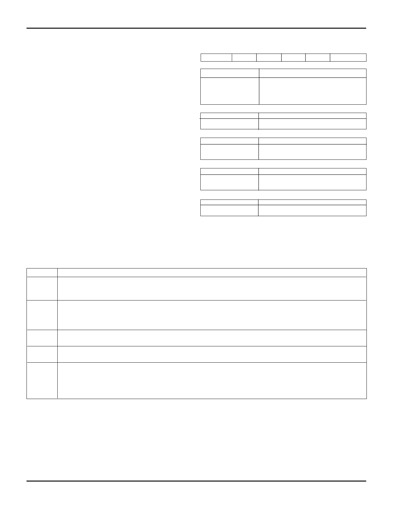
MODE REGISTER CONFIGURATION
15
76
5
4
32
0
UNUSED RMODE PSEL RWBD CLEAR EDCM0-2
EDCM2 EDCM1 EDCM0
0
0
0
0
0
1
0
1
0
0
1
1
1
0
0
OPERATION
ERROR-DATA OUTPUT MODE
DIAGNOSTIC-OUTPUT MODE
GENERATE-DETECT MODE
NORMAL MODE
CHECKBIT-INJECTION MODE
RMODE
0
1
OPERATION
NOP
READ MODE REGISTER ON SD BUS
RWBD
0
1
OPERATION
DUAL FIFOS (8)
SINGLE FIFO (16)
CLECARLEAR
0
1
OPERATION
NOP
CLEAR ALL DIAGNOSTIC REGISTERS
PSEL
0
1
OPERATION
EVEN PARITY
ODD PARITY
2617drw 06
OPERATING MODE DESCRIPTION
Mode
Description
MODE 0
Error-Data Output Mode: This mode allows the uncorrected data captured from an error event by the Error-Data
Register to be read by the system for diagnostic purposes. The Error-Data Register is cleared by setting the mode
register "'clear"-bit.
MODE 1
Diagnostic-Output Mode: In this mode, contents of latch and five internal registers are read by the system for
diagnostic and error logging purposes. Internal data paths allow output from the CBI LATCH to be read directly by the
system bus for diagnostic purposes. The contents of the internal diagnostic checkbit register, syndrome registers, error
count register and error-type register are also output on the SD bus.
MODE 2
Generate-Detect Mode: (Detect-Only) The EDC performs checkbit generation during a memory write, and performs
error detection only during a memory read.
MODE 3
Normal Mode: The EDC performs checkbit generation during memory writes and error detection and correction during
memory reads.
MODE 4
Checkbit-Injection Mode: In this mode, the checkbit latch is loaded with desired 8-bit data from the SD bus.This eight
bit data passes through SD Latch in or write FIFO to the MD check bit latch. By inserting various checkbit values,
correct functioning of the EDC can be verified “on-board”. The rest of the operation is similar to regular memory
reads. The EDC compares the injected checkbits against the internally generated checkbits. Any discrepancy in the
injected checkbits and the internally generated checkbits will cause the ERR / MERR to go LOW.
2617 tbl 08
Memory Initialization
Memory initialization involves clearing all memory data locations and writing the corresponding checkbits (checkbits
corresponding to all zero data = $0C) to checkbit memory. This can be done using the 49C466 to first create an "all-zero-data"
source. This is done by setting the CLEAR bit in the mode register. This clears all diagnostic registers. Then this data can
be written back to memory in the Error-Data output (Mode 0) mode. In order to wrap the all-zero data back to the MD bus, BE0-
7 should be high and WBSEL =0.
11.7
10