MSK5021(2015) Ver la hoja de datos (PDF) - M.S. Kennedy Corporation
Número de pieza
componentes Descripción
Fabricante
MSK5021
(Rev.:2015)
(Rev.:2015)
M.S. Kennedy Corporation

MSK5021 Datasheet PDF : 7 Pages
| |||
ABSOLUTE MAXIMUM RATINGS 9
VIN Input Voltage
VEN Enable Voltage
IOUT Output Current
TJ Junction Temperature
36V
-0.3V to 36V
20A within SOA
+175°C
TST Storage Temperature Range 11
TLD Lead Temperature Range
(10 Seconds)
TC Case Operating Temperature
MSK5021
MSK5021B Series
-65°C to +150°C
300°C
-40°C to +85°C
-55°C to +125°C
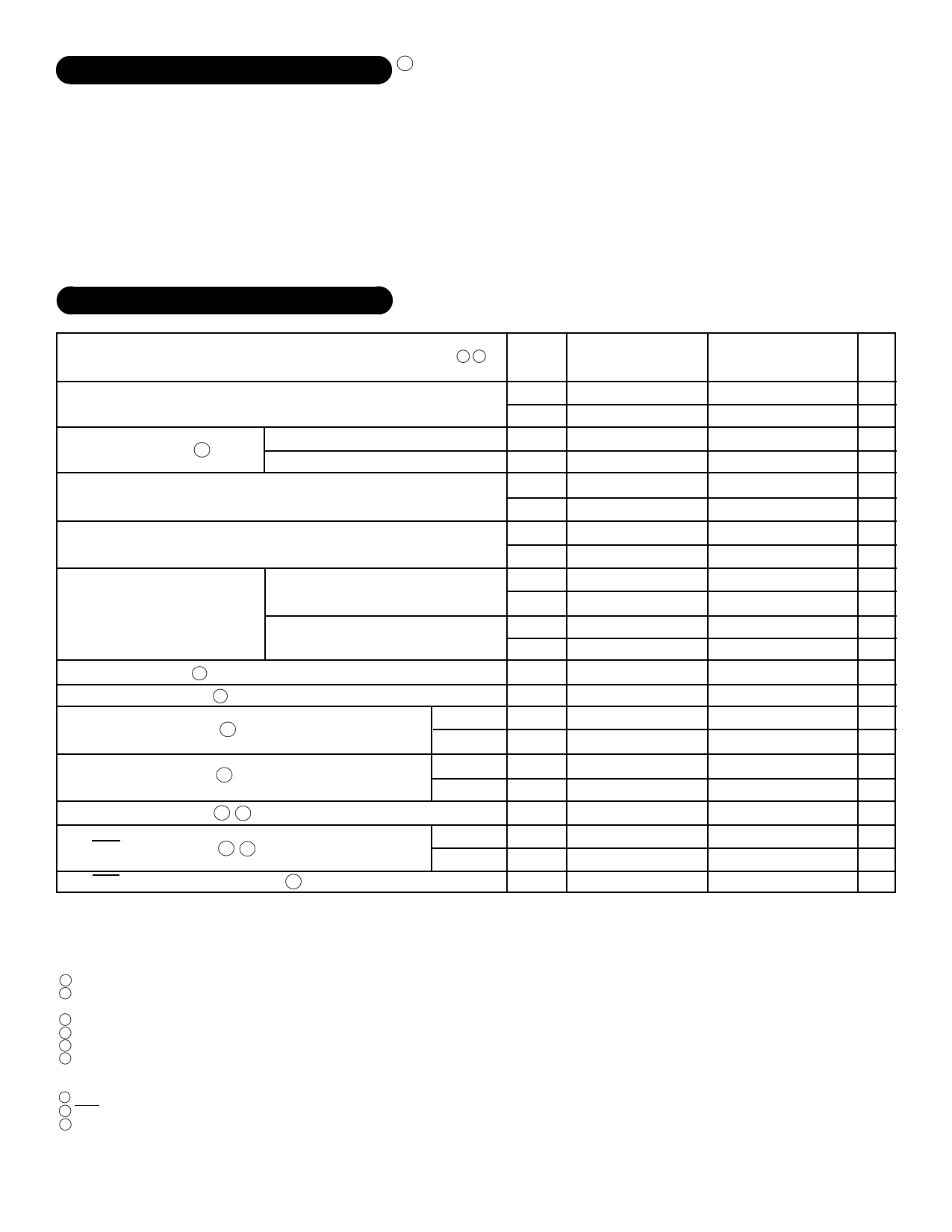
ELECTRICAL SPECIFICATIONS
Parameter
Input Voltage Range
2
Output Voltage Tolerance 2 9
VAdjust Voltage
Dropout Voltage 2
Load Regulation
Line Regulation
Quiescent Current
Ripple Rejection 2
Thermal Resistance 2
Enable Input Voltage 2
Enable Input Current 2
Output Settling Time 2 7
Fault Output Voltage 2 8
Fault Output Sink Current Range
Test Conditions 1 3
IOUT=0A; VIN=VOUT+1V
IOUT= 0A
IOUT=20A
VIN=VOUT+1V
0A ≤ IOUT ≤ 10A
(VOUT +1V) ≤ VIN ≤ (VOUT+15V)
IOUT=0A
VEN=5V; VIN=VOUT+1V; IOUT=0A
VEN=0V; VIN=VOUT+1V; IOUT=0A
f=120Hz
Junction to Case @ 125°C
HIGH
LOW
HIGH
LOW
To within 10mV (IOUT=0A)
IFAULT=1mA
HIGH
LOW
Group A
MSK5021B
Subgroup Min. Typ. Max. Min.
-
3
-
36 3
1
-
±0.5 ±1.0 -
2,3
-
±1.0 ±2.0 -
1 1.222 1.235 1.248 1.21
2,3 1.211
-
1.259 -
1
-
0.002 0.010 -
1
-
0.50 0.75 -
1
-
±0.5 ±1.0 -
2,3
-
±0.5 ±2.0 -
1
-
±0.5 ±1.0 -
2,3
-
±0.5 ±1.0 -
1
-
20
30 -
2,3
-
20
30 -
1
-
10
50 -
2,3
-
10
50 -
-
2.4
45
-
-
-
-
0.8
1.0 -
1
-
1.2
- 2.4
1
-
1.2
0.8 -
1
-
20
50 -
1
-
10
25 -
-
-
0.5
-
-
-
1
VIN
-
-
-
-
0.09
-
-
-
-
-
10 1
MSK5021
Typ. Max. Units
-
36 V
±0.5
±1.0 %
-
-%
1.24
1.26 V
-
-
V
0.002 0.010 V
0.5
1.0 V
±0.5
±1.0 %
-
-%
±0.5
±1.0 %
-
-%
20
30 mA
-
- mA
10
50 µA
-
- µA
45
- dB
0.8
1.0 °C/W
1.2
-
V
1.2
0.8 V
20
50 µA
10
25 µA
0.5
- mS
VIN
-
V
0.09
-
V
-
10 mA
NOTES:
1 Output decoupled to ground using 33µF minimum capacitor and RSC=0Ω unless otherwise specified.
2 This parameter is guaranteed by design but need not be tested. Typical parameters are representative of actual device perfor-
mance but are for reference only.
3 All output parameters are tested using a low duty cycle pulse to maintain TJ = TC.
4 Industrial grade devices shall be tested to subgroup 1 only unless otherwise specified.
5 Military grade devices ('B' suffix) shall be 100% tested to subgroups 1,2 and 3.
6 Subgroup 1
TA=TC=+25°C
Subgroup 2
TA=TC=+125°C
Subgroup 3
TC=TC=-55°C
7 After application of enable pulse.
8 Fault pin connected to VIN through a 5.1KΩ resistor for VIN=5.0V.
9 Does not include tolerance effects from external resistor
10 Continuous operation at or above absolute maximum ratings may adversly effect the device performance and/or life cycle.
11 Internal solder reflow temperature is 180°C, do not exceed.
2
8548-153 Rev. J 5/15
Share Link: