MPC2005 Ver la hoja de datos (PDF) - Motorola => Freescale
Número de pieza
componentes Descripción
Fabricante
MPC2005
Motorola => Freescale

MPC2005 Datasheet PDF : 6 Pages
| |||
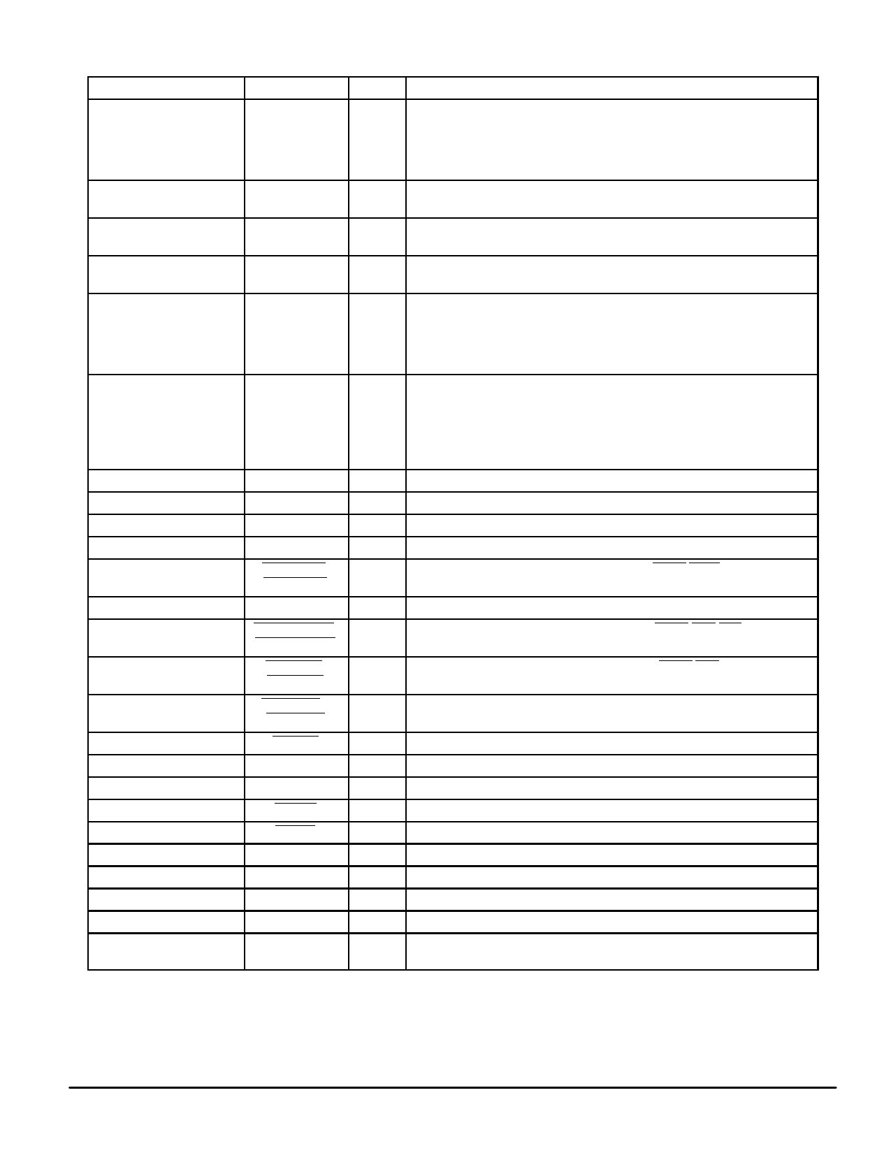
PIN DESCRIPTIONS
Pin Locations
68, 69, 70, 71, 73, 74, 75,
76, 78, 79, 80, 82, 83, 84,
85, 159, 160, 161, 162,
164, 165, 166, 167, 169,
170, 171, 173, 174, 175
62, 63
153, 154
30, 56, 117, 146, 148
Symbol
A0 – A28
ADDR0A,
ADDR0B
ADDR1A,
ADDR1B
CLK0 – CLK4
4, 5, 6, 7, 10, 11, 12, 14,
16, 17, 19, 20, 22, 24, 25,
26, 27, 95, 96, 97, 98, 101,
102, 103, 105, 107, 108,
110, 111, 113, 115, 119
32, 33, 34, 37, 38, 39, 40,
43, 44, 45, 47, 49, 50, 52,
53, 54, 121, 122, 124, 125,
126, 129, 130, 131, 133,
135, 136, 138, 139, 141,
143, 144
9, 15, 21, 28, 35, 42, 48, 58
3, 94
2
93
64, 65
151
155, 156
59, 60
100, 106, 112, 120, 128,
134, 140, 150
87
88
178
179
89
90
181
180
176
8, 23, 51, 61, 77, 99, 114,
142, 152, 168
DH0 – DH31
DL0 – DL31
DP0 – DP7
PD2, PD3
PD0/IDSCLK
PD1/IDSDATA
SRAMADS0,
SRAMADS1
SRAM ALE
SRAMCNTEN0,
SRAMCNTEN1
SRAMOE0,
SRAMOE1
SRAMWE0 –
SRAMWE7
TAGCLR
TAG MATCH
TAG VALID
TAGWE
TAGOE
DIRTYIN
DIRTYOUT
STANDBY
RESERVED
VCC3
Type
Input
Description
Address Inputs – (MSB:0, LSB:28)
Input Least significant address bit when asynchronous SRAMs are used.
Input Next to least significant address bit when asynchronous SRAMs are used.
Input
I/O
Clock Inputs – CLK2 is for Tag RAM, CLK0, 1, 3, and 4 are for SRAMs.
For 1MB use all the clocks. For 512KB or less us CLK0–CLK2 only.
High Data Bus – (MSB:0, LSB:31)
I/O Low Data Bus – (MSB:0, LSB:31)
I/O
Output
Input
I/O
Input
Data Parity Bus – (MSB:0, LSB:7)
Presence detect bits 2 and 3.
Presence detect bit 0/EEPROM serial clock.
Presence detect bit 1/EEPROM serial data.
SRAM Address Strobe – For 512KB or less us SRAM ADS0 only.
Input
Input
SRAM Address Latch Enable – Use for asynchronous SRAM only.
SRAM Count Enables – For 512KB or less use SRAM CNT EN0 only.
Input SRAM Output Enables – For 512KB or less use SRAM OE0 only.
Input SRAM Write Enables – (MSB:0, LSB:7)
Input
Output
Input
Input
Input
Input
Output
Input
Input
Tag RAM clear.
Tag RAM match indication.
Tag RAM valid bit.
Tag RAM write enable.
Tag RAM output enable.
Dirty input bit.
Dirty output bit.
Standby pin. Reduces standby power consumption.
Reserved pin.
+ 3.3 V power supply.
MOTOROLA FAST SRAM
MPC2004•MPC2005
6–5
Share Link: