MP2105(2005) Ver la hoja de datos (PDF) - Monolithic Power Systems
Número de pieza
componentes Descripción
Fabricante
MP2105 Datasheet PDF : 8 Pages
| |||
TM
MP2105 – 1MHz 800mA SYNCHRONOUS STEP-DOWN CONVERTER
Manufacturer
Coilcraft
Toko
Sumida
Table 2—Suggested Surface Mount Inductors
Part Number
D01605T-472
D52LC
CR43-4R7
Inductance (µH)
4.7
4.7
4.7
Max DCR (Ω)
0.150
0.087
0.109
Saturation
Current (A)
1.20
1.14
1.15
Dimensions
LxWxH (mm3)
5.4x4.2x1.8
5x5x2
4.3x4.8x3.5
Table 3—Inductors for Improved Efficiency at 25mA, 50mA, under 100mA Load.
Manufacturer
Coilcraft
Murata
Sumida
Sumida
Part Number
DO1605T-103MX
LQH4C100K04
CR32-100
CR54-100
Inductance (µH)
10
10
10
10
Max DCR (Ω)
0.3
0.2
0.2
0.1
Saturation
Current (A)
1.0
1.2
1.0
1.2
IRMS (A)
0.9
0.8
0.7
1.4
Input Capacitor Selection
The input capacitor reduces the surge current
drawn from the input and switching noise from
the device. The input capacitor impedance at
the switching frequency shall be less than input
source impedance to prevent high frequency
switching current passing to the input. Ceramic
capacitors with X5R or X7R dielectrics are
highly recommended because of their low ESR
and small temperature coefficients. For most
applications, a 4.7µF capacitor is sufficient.
Output Capacitor Selection
The output capacitor keeps output voltage
ripple small and ensures regulation loop stable.
The output capacitor impedance shall be low at
the switching frequency. Ceramic capacitors
with X5R or X7R dielectrics are recommended.
The output ripple ∆VOUT is approximately:
( ) ∆VOUT
≤
VOUT × VIN − VOUT
VIN × fOSC × L
×
⎜⎜⎝⎛ESR
+
8
×
1
fOSC
×
C3
⎟⎟⎠⎞
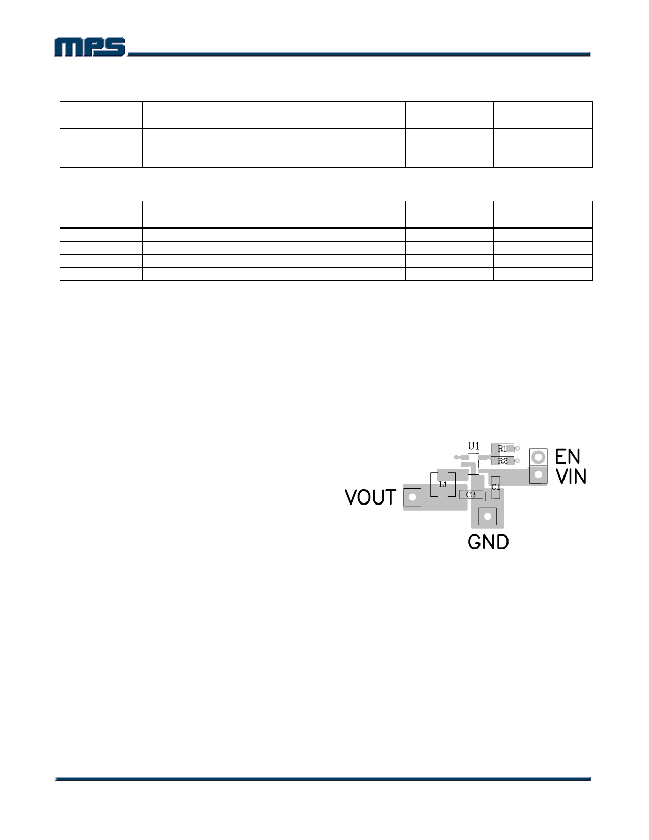
PC Board Layout
The high current paths (GND, IN and SW)
should be placed very close to the device with
short, direct and wide traces. Input capacitor C1
needs to be as close as possible to the IN and
GND pins. The external feedback resistors shall
be placed next to the FB pin. Keep the
switching node SW short and away from the
feedback network. Figure 2 illustrates an
example of PCB layout and signal routing.
Figure 2—MP2105 Suggested Layout
MP2105 Rev. 1.2
www.MonolithicPower.com
7
8/19/2005
MPS Proprietary Information. Unauthorized Photocopy and Duplication Prohibited.
© 2005 MPS. All Rights Reserved.
Share Link: 