MM5450 Ver la hoja de datos (PDF) - Micrel
Número de pieza
componentes Descripción
Fabricante
MM5450 Datasheet PDF : 9 Pages
| |||
Micrel, Inc.
MM5450/5451
Absolute Maximum Ratings
Voltage (any pin) ........................................VSS to VSS + 12V
Power Dissipation
+25°C ........................................................................ 1W
+85°C.................................................................560mW
Junction Temperature (TJ) ....................................... +150°C
Storage Temperature (TS).........................–65°C to +150°C
Lead Temperature (soldering, 10sec.) ..................... +300°C
Operating Ratings
Supply voltage (VDD – VSS).......................... +4.75V to +11V
Ambient Temperature Range (TA) ............. –40°C to +85°C
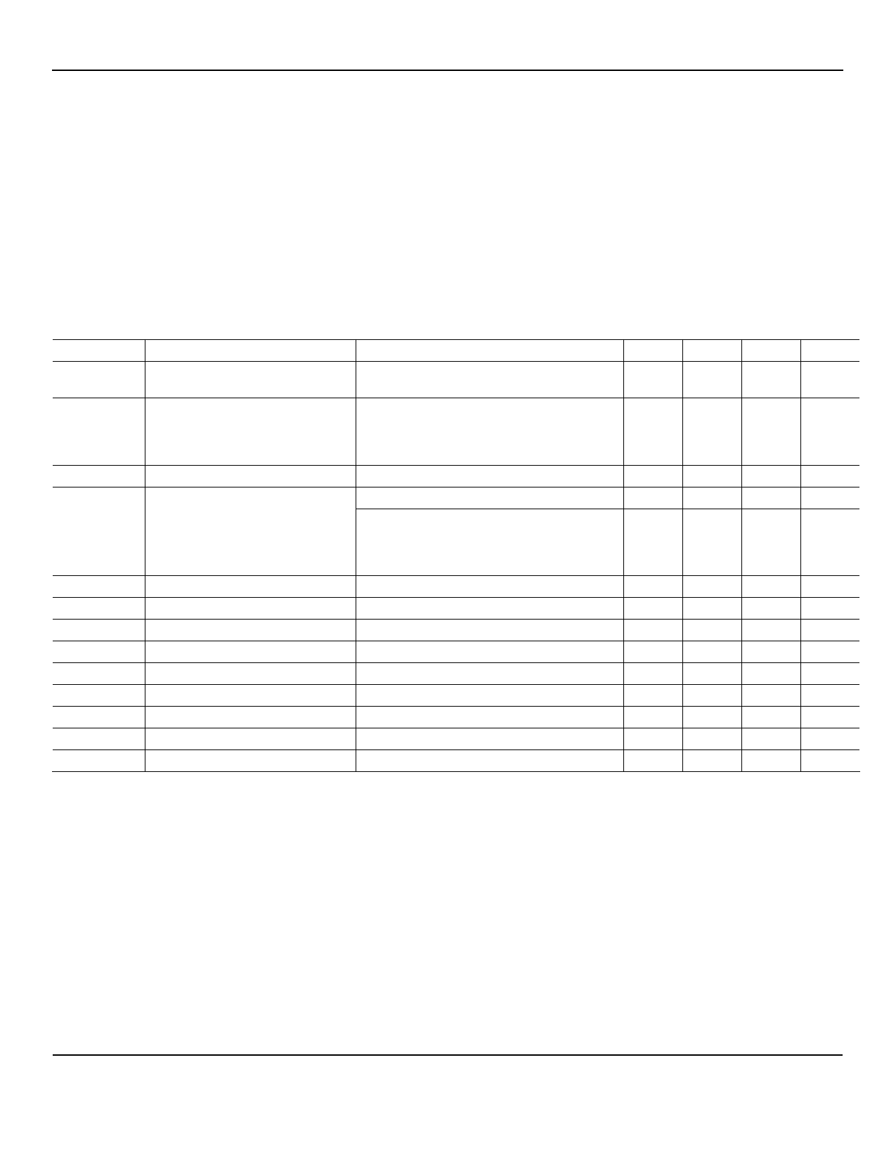
Electrical Characteristics
4.5V ≤ VDD ≤ 11V, VSS = 0V; TA = 25°C, bold values indicate –40°C ≤ TA ≤ +85°C, unless otherwise noted.
Symbol
Parameter
Condition
Min
Typ
Max
Power Supply Current
–25°C to +85°C, excluding output loads
8.5
–40°C to +85°C, excluding output loads
10
Data Input Voltage
VL
VH
logic-0 level, ±10 µA input bias
–0.3
0.8
logic-1 level, 4.75V ≤ VDD ≤ 5.25V
2.2
VDD
VDD > 5.25V
VDD –2
VDD
Brightness Control Input Current Note 2
0
0.75
Output Sink Current
segment off, VOUT = 3.0V
10
segment on, VOUT = 1.8V, Note 3
brightness input = 0µA
brightness input = 100µA
brightness input = 750µA
0
10
2.0
2.7
4
15
25
Brightness Control Input Voltage input current = 750 µA
3.0
4.3
Output Matching
Note 1
±20
fC
Clock Input Frequency
Notes 5, 6
tH
Clock Input High Time
Notes 5, 6
500
950
tL
Clock Input Low Time
Notes 5, 6
950
tDS
Data Input Setup Time
300
tDH
Data Input Hold Setup Time
300
tDES
Data Enable Input Setup Time
100
Reset Pad Current
die
8
8
Notes:
1. Output matching is calculated as the percent variation (IMAX + IMIN) / 2.
2. With a fixed resistor on the brightness input pin, some variation in brightness will occur among devices.
3. See Figures 7, 8 and 9 for recommended operating conditions and limits. Absolute maximum for each output should be limited to 40mA.
4. VOUT should be regulated by user. See Figures 8 and 9 for allowable VOUT vs. IOUT operation.
5. AC input waveform specification for test purpose: tR ≤ 200ns, tF ≤ 20ns, f = 500kHz, 50% ±10% duty cycle.
6. Clock input rise and fall times must not exceed 300ns.
Units
mA
mA
V
V
V
mA
µA
µA
mA
mA
V
%
kHz
ns
ns
ns
ns
ns
µA
February 2006
4
M9999-021606
(408) 955-1690
Share Link: 