MM1106 Ver la hoja de datos (PDF) - Mitsumi
Número de pieza
componentes Descripción
Fabricante
MM1106 Datasheet PDF : 5 Pages
| |||
MITSUMI
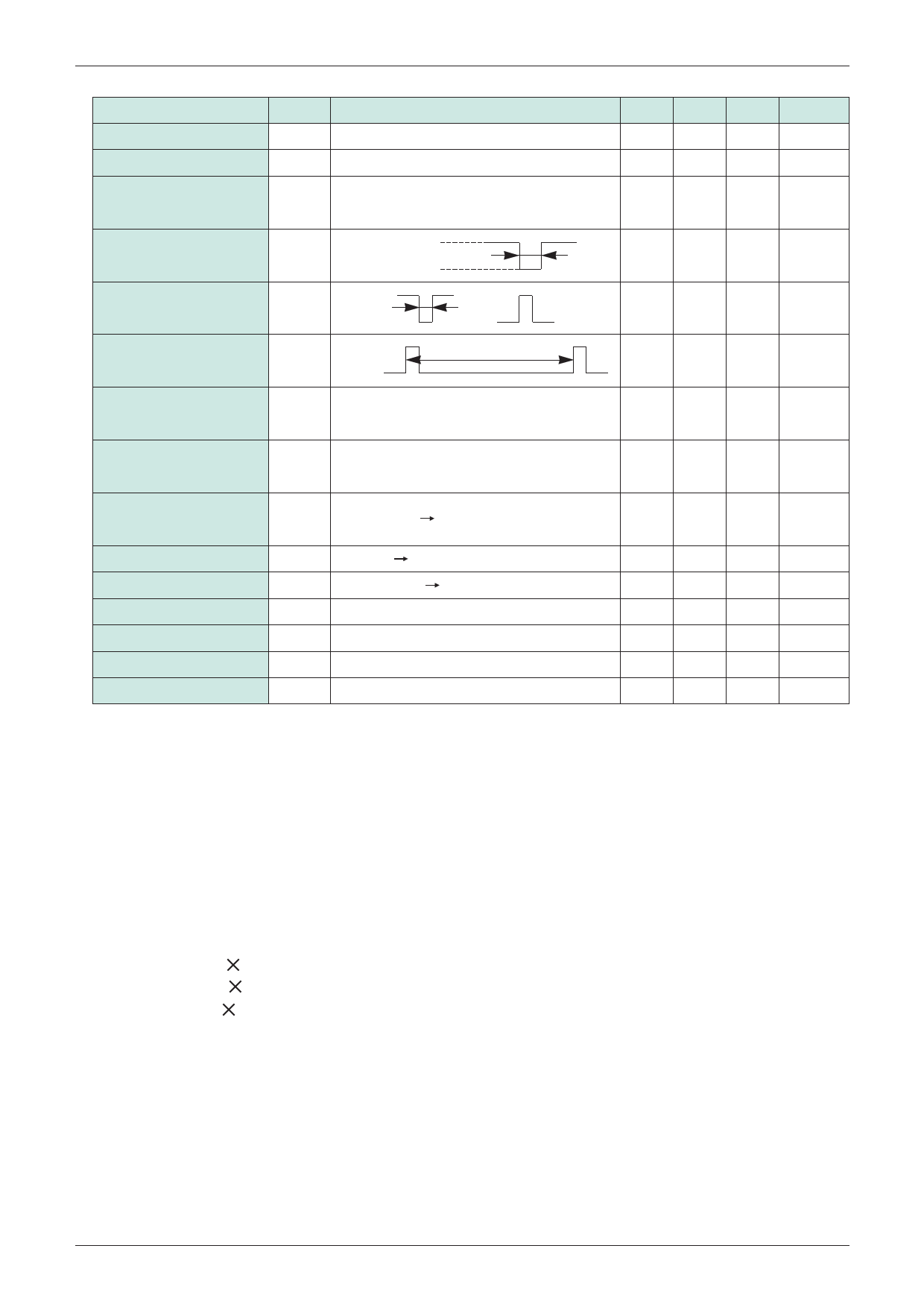
System Reset (with watchdog timer+battery back-up) MM1106
Item
Symbol
Loss current
ILOSS
Reverse current
IOREV
External PNP transistor
IBASE
base-driving current
VCC input pulse width TPI
Measurement conditions
VCC=0V, IO=0µA, VBAT=3V
VCC=5.0V, IO=0µA, VBAT=0V
VCC=5.0V, VOUT=4.2V, VTB=4.3V
5.0V
VCC
4.0V
Min. Typ. Max.
0.1
0.1
Units
µA
µA
2
5
mA
8
µS
CK input pulse width TCKW CK
tCKW or
20
µS
tCk
CK input cycle
TCK CK
20
µS
Watchdog timer
TWD
* monitoring time 1
CT=0.02µF
50 100 150 mS
Watchdog timer
TWR
* reset time 2
CT=0.02µF
1
2
3
mS
Reset hold time for
TPR
VCC : Lo Hi (100µS), CT=0.02µF
50 100 150 mS
* power supply rise 3
---------------------------------------------
RESET delay time
TPDR VCC : Hi Lo (50µS), CLR=15pF, RLR=22kΩ
10
µS
CS delay time
--------------------------------------------
RESET rise time
--------------------------------------------
RESET fall time
TPDC
TRR
TFR
VCC : Hi Lo (50µS), CLC=15pF
CLR=15pF, RLR=22kΩ
CLR=15pF, RLR=22kΩ
10
µS
4
µS
4
µS
CS rise time
TRC
CLC=15pF
4
µS
CS fall time
TFC
CLC=15pF
4
µS
Notes:
*1 Monitoring time is the time from the last pulse (negative edge) of the timer clear clock pulse until reset
pulse output. In other words, reset output is output if a clock pulse is not input during this time.
*2 Reset time means reset pulse width. However, this does not apply to power ON reset.
*3 Reset hold time is the time from when VCC exceeds detection voltage (VSHR) during power ON reset until
------------------------------------------------
reset release (RESET output high).
*4 Watchdog timer monitoring time (TWD), watchdog timer reset time (TWR) and reset hold time (TPR) during
power supply rise can be changed by varying CT capacitance. The times are expressed by the following
formulae.
Example : when CT=0.02µF
TPR (mS) .=. 5000 CT (µF)
TWD (mS) .=. 5000 CT (µF)
TWR (mS) .=. 100 CT (µF)
TPR .=. 100mS
TWD .=. 100mS
TWR .=. 2mS
*5 The voltage range when measuring output rise and fall time is 10~90%.
*6 The IC can be made to operate only as a reset IC with delay during Vcc rise by connecting the RCT pin to
GND.
*7 VCC rise time should be 100µS or more, and fall time should be 50µS or more.
Share Link: 