EM19110 Ver la hoja de datos (PDF) - ELAN Microelectronics
Número de pieza
componentes Descripción
Fabricante
EM19110 Datasheet PDF : 6 Pages
| |||
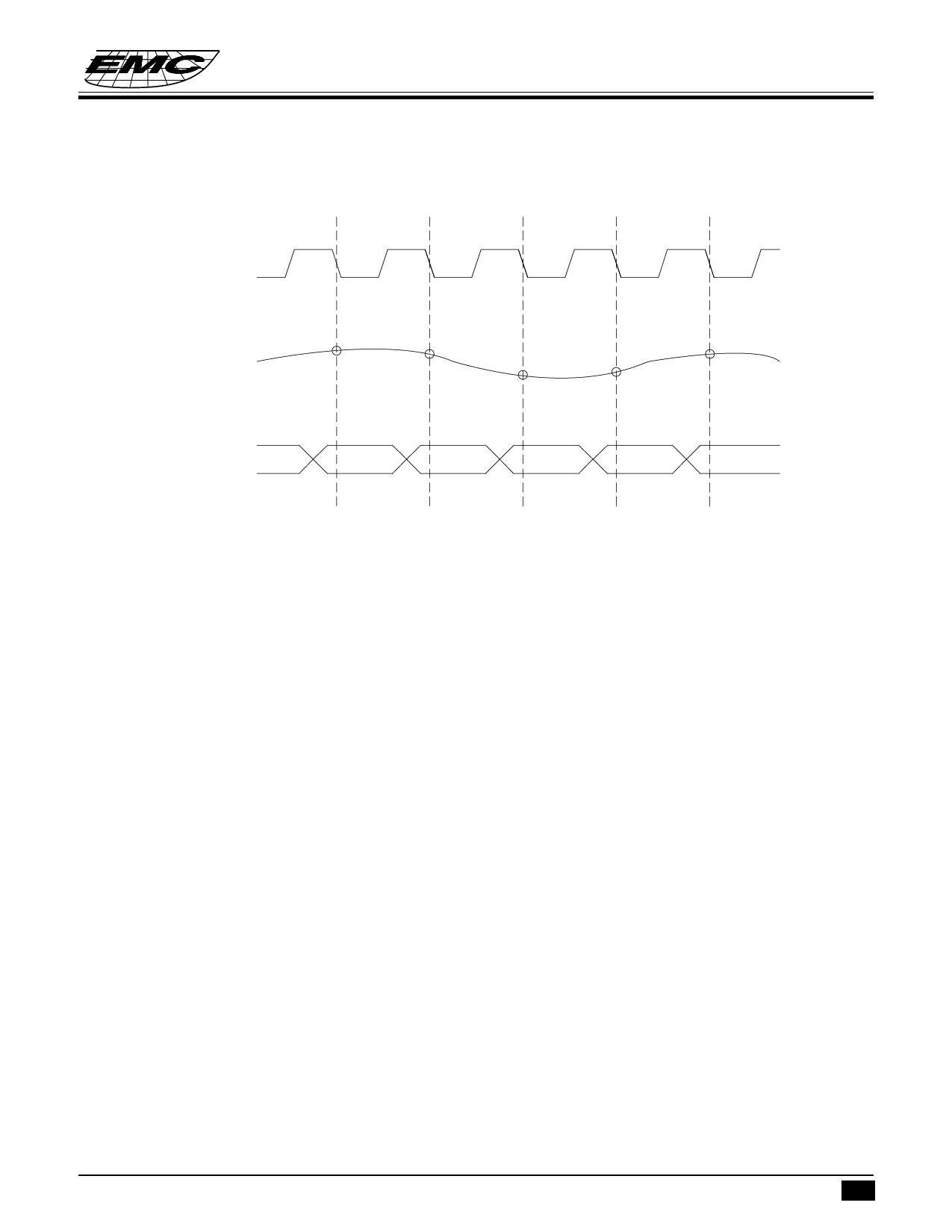
TIMING DIAGRAM
Clock
Analog input
Data output
EM19110
10-BIT 5 MSPS A/D CONVERTER
N
N+1
N+2
N+3
N-3
N-2
N-1
N
N+4
N+1
Application Note
1. AVDD ,DVDD ,VSS
To reduce noise effects, separate the analog and digital systems close to the device. For both the digital and
analog VDD pins, use a ceramic capacitor of about 0.1uF set as close as possible to the pin to bypass to the
respective GND’s.
2. Signal input Vi
Compared with the flash type A/D converter, the input capacitance of the analog input is rather small. However
it is necessary to conduct the drive with an amplifier featuring sufficient band and drive capability. When
driving with an amplifier of low output impedance, parasite oscillation may occur. That may be prevented by
inserting a resistance of about 100( in series between the amplifier output and A/D input.
3. Clock input
The clock line wiring should be as short as possible also, to avoid any interference with other signals, separate
it from other circuits.
4. Reference voltage
Voltage between VRT to VRB is compatible with the dynamic range of the analog input. Bypassing VRT and
VRB pins to GND, by means of a capacitor about 0.1uF, stable characteristics are obtained. By shorting VRT
and VRTS, VRB and VRBS, the self bias function that generates VRT=4.0V and VRB=1.0V, is activated.
Also, the users can setup external reference voltage by just connecting VRT and VRB to desired DC voltage
under spec.
5. Clock timing
* This specification are subject to be changed without notice.
5.26.1997 4
Share Link: 