ML9209 Ver la hoja de datos (PDF) - Oki Electric Industry
Número de pieza
componentes Descripción
Fabricante
ML9209 Datasheet PDF : 29 Pages
| |||
OKI Semiconductor
FEDL9209-01
ML9209-xx
FUNCTIONAL DESCRIPTION
Command List
Command
LSB
First byte
MSB LSB
Second byte
MSB
B0 B1 B2 B3 B4 B5 B6 B7 B0 B1 B2 B3 B4 B5 B6 B7
1 DCRAM data write X0 X1 X2 X3 1 0 0 0 C0 C1 C2 C3 C4 C5 C6 C7
C0 C1 C2 C3 C4 C5 C6 C7 2nd byte
2 CGRAM data write X0 X1 X2 X3 0 1 0 0
C8 C9 C10 C11 C12 C13 C14 C15 3rd byte
XXXX
3 ADRAM data write 0 1 2 3 1 1 0 0 C0 C1 * * * * * *
5 Display duty set
D0 D1 D2 D3 1 0 1 0
6 Number of digits set K0 K1 K2 K3 0
1
1
0
* : Don’t care
Xn : Address setting for each RAM
7
All display lights
ON/OFF
L H * * 1 1 1 0 Cn : Character code setting for each RAM
Dn : Display duty setting
Others (test mode)
Kn : Setting of the number of display digits
H : All display lights ON setting
L : All display lights OFF setting
When data is written to RAM (DCRAM, CGRAM, and ADRAM) continuously, addresses are internally
incremented automatically. Therefore it is not necessary to specify the 1st byte to write RAM data for the 2nd
and subsequent bytes.
Note: The test mode is used for inspection before shipment. It is not a user function.
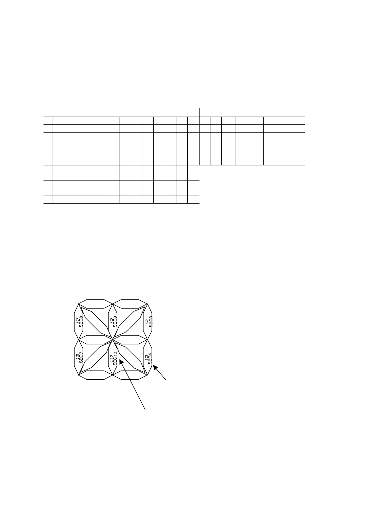
Positional Relationship Between SEGn and ADn (one digit)
C0
SEG1
C1
SEG2
C15
SEG16
C9
SEG10
C14
SEG15
C13
SEG14
C10
SEG11
C11
SEG12
C5
SEG6
C4
SEG5
C0–7: Corresponds to the 2nd byte of the CGRAM data write
command.
C8–15: Corresponds to the 3rd byte of the CGRAM data write command.
11/29
Share Link: 